In this tutorial we will go through I2C Bus & Protocol. I2C was originally invented by Philips(now NXP) in 1982 as bi-directional bus to communicate with multiple devices using just 2 wires/lines. I2C stands for Inter-Integrated Circuit. I2C is sometimes also referred as TWI, which is short for Two Wire Interface, since it uses only 2 wires for data transmission and synchronization. I2C is pronounced and referred to as “I-Squared-C” [I2C] , “I-Two-C” [I2C] and “I-I-C” [IIC]. The two wires of I2C Bus consists of:
1. Data Line called SDA which is short for Serial Data
2. Clock Line called SCL which is short for Serial Clock
SDA is the wire on which the actual data transfer happens, which is bi-directional, between different masters and slaves. SCL is the wire on which the Master device generates a clock for slave device(s).
I2C supports 7 bit and 10 bit addresses for each device connected to the bus. 10 bit addressing was introduced later. With 7 bit address its possible to connect up to 128 I2C devices to the same bus, however, some addresses are reserved so practically only 112 devices can be connected at the same time. With 10 bit address a maximum of 1024 devices can be connected. To keep things simple we will be going through 7 bit addressing in this tutorial. For 10 bit addressing you can look up the official I2C specification by NXP, a link to which is given at the bottom of this tutorial. Once you get familiar with the I2C protocol, 10 bit addressing will be a piece of cake.
As per the original specification of I2C/TWI, it supports a maximum frequency of 100Khz. But along the years the specifications was updated many times and now we have a bunch of different speed modes. The latest mode added was Ultra-Fast Mode which allows I2C bus transfer speeds of up to 5Mhz.
| I2C Speed Mode | I2C Speed | Communication |
|---|---|---|
| Standard Mode (Sm) | 100 Kbit/s [Khz] | Bidirectional |
| Fast Mode (Fm) | 400 Kbit/s [Khz] | Bidirectional |
| Fast Mode Plus (Fm+) | 1 MBits/s [Mhz] | Bidirectional |
| High-speed mode (Hs-mode) | 3.4 MBits/s [Mhz] | Bidirectional |
| Ultra Fast-mode (UFm) | 5 MBits/s [Mhz] | Unidirectional |
I2C has 4 operating modes:
- Master Transmitter mode : Master Writes Data to Slave
- Master Receiver mode : Master Reads Data from Slave
- Slave Transmitter mode : Slave Write Data to Master
- Slave Receiver mode : Slave Reads Data from Master
Even though multiple masters may be present on the I2C bus the arbitration is handled in such a way that there is no corruption of data on bus in case when more than 2 masters try to transmit data at the same time. Since the transmission, synchronization and arbitration is done using only 2 wires on the bus, the communication protocol might be a bit uneasy to understand for beginners .. but its actually easy to understand – just stick with me 🙂
A general I2C/TWI bus topology with multiple masters and multiple slaves connected to the bus at the same time is shown below:

Let us go through I2C protocol basics first. I2C bus is a Byte Oriented bus. Only a Byte can be transferred at a time. Communication(Write to & Read from) is always initiated by a Master. The Master first sends a START condition and then writes the Slave Address (SLA) and the Direction bit(Read=1/Write=0) on bus and the corresponding Slave responds accordingly.
Format for I2C communication protocol

-
Case 1 – Data transfer from “Master transmitter” to “Slave receiver”
- In this case, after sending the START condition, the Master sends the First Byte which contains the Slave address + Write bit.
- The corresponding slave acknowledges it by sending back an Acknowledge (ACK) bit to the Master.
- Next, the Master sends 1 or more bytes to slave. After each byte received the Slave sends back an Acknowledge bit (ACK).
- When Master wants to stop writing it then sends a STOP condition.
-
Case 2 – Data transfer from “Slave transmitter” to “Master receiver”
- Here the Master sends the First Byte which contains the Slave address + Read bit
- The corresponding Slave acknowledges it by sending back an Acknowledge (ACK) bit to the Master.
- Next, the Slave sends 1 or more bytes and the Master acknowledges it everytime by sending an Acknowledge bit (ACK).
- When the Master wants to stop reading it sends a Not Acknowledge bit (NACK) followed by a STOP condition.
Format for first byte after START
As soon as the START condition is transmitted on the bus, the first byte (or the control byte) is transmitted. Bits 7 to 1 contain the Slave address and Bit 0 is direction(Read/Write) bit.

An example of timing diagram for complete data transfer
Given below, is a timing diagram for complete transfer of 3 Bytes including the first byte:

Image Source: I2C Specification
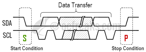
Start & Stop Conditions
All I2C transactions begin with a START (S) and are terminated by a STOP (P).
START condition : When a HIGH to LOW transition occurs on the SDA line while SCL is HIGH.
STOP condition : When a LOW to HIGH transition occurs on the SDA line while SCL is HIGH.

Repeated Start
A Repeat Start condition is similar to a Start condition, except it is sent in place of Stop when the master does not want to loose the control over the bus and wants to complete its transfers in atomic manner when multiple masters are present. When a master wants to switch to Master Receiver Mode from Master Transmitter mode or vice-versa it sends a Repeated start at the end of the current transfer so it remains master when next transfer starts.

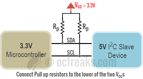
SDA & SCL Voltage levels for different Voltage devices on same bus
In many cases(but not all!), I2C supports devices having different signal voltage levels to be connected to the same bus. Like for example interfacing 5V I2C Slave device with a 3.3V microcontroller like lpc1768, lpc2148 or interfacing 3.3V I2C Slave device with 5V microcontroller like Arduino. In such cases we connect the Pull-up resistors to the lower of the Vcc/Vdd. In the mentioned examples it would be 3.3V in both cases since its the lower one. As per the I2C specification Input reference levels are set as 30 % and 70 % of Vcc. Hence, VIL(LOW-level input voltage) is 0.3Vcc and VIH(HIGH-level input voltage) is 0.7Vcc. If these thresholds for Input Reference Levels are met when using two or more device with different voltages you are good to go by connecting pull ups to lowest Vcc else you will need a line buffer/driver which provides level-shifting, between the different voltage level devices based on CMOS, NMOS, TTL, etc.

Opendrain SDA and SCL lines
I2C uses Open-drain / Open-Collector drivers for both SDA and SCL. Consider the following image showing basic open-drain driver for I2C:

Here the buffer is used to Receive(input) data and Mosfet is used to Transmit(output) data. Drivers for both SDA and SCL are similar. When the Mosfet is activated it will sink the current from pull-ups resistors which forces the pin to a Logic Low. Note that it cannot drive the line to HIGH by itself which is obvious. To provide a logic High state when the output driver is not trying to pull the line LOW we use Pull-Up resistors. Using pull-ups the logic state of SDA and SCL signals on the I2C bus is always defined and never floating(digitally). Hence, when no transfers are occurring and the bus is idle, SDA and SCL are continuously pulled to logic high.
I2C Pull-Up Resistor Values
We will go into intricacies of Pull up resistor Value selection for a particular mode in another post since its a function of bus capacitance and Vcc/Vdd along with sinking current. For beginners it better to following the rule of thumb: You need lower resistor values as the speed increases and Vice-versa. For simple general purpose projects/application you can use a pull-up resistor value between 1kΩ to 10kΩ. For example when interfacing I2C devices at 100Khz I use 10kΩ pull ups.
Clock Stretching
Clock Stretching is a mechanism for slave devices to make the master wait until data is ready or slave device has to finish some internal operations (like: ADC conversion, Initial internal Write cycle, etc..) before proceeding further. In Clock Stretching the SCL line is held low by the slave which pauses the current transfer.

Acknowledge Polling
In practice, many Slave devices do not support clock stretching. Consider 24c16, at24c32, 24lc256, etc. series of EEPROMs. These devices do not support clock stretching even though they have to perform internal byte write or page write operation when the master does a write operation. In this case the master has to initiate an Acknowledge Polling (for EEPROMs its also called Write Polling) which checks if the EEPROM has finished internal operation or not. When the EEPROM starts internal write cycle it won’t respond to its address but when it completes, it responds with an ACK to the master. So, in Acknowledge Polling we keep on sending the slave address with write bit and wait for any ACK from the Slave which indicates Slave is ready for next operation.
Condition for Valid Data (Data Validity)
For any data bit to be Valid, the SDA line must be stable when the period of clock is HIGH. The change in state of the SDA line(From HIGH to LOW or Vice-versa) can only happen when the SCL line is LOW. A valid data bit is transferred for each corresponding clock pulse. This is illustrated in the timing diagram shows below:

I2C Master Modes when using Microcontrollers / Arduino
When interfacing Microcontrollers, like LPC2148, LPC1768, LPC1114, Atmega8/16, PICs or MCU Boards like Arduino Uno (Atmega 168/368) or Raspberry Pi, generally we use Master Transmitter & Master Receiver mode since we interface such MCUs with Slave-Only I2C devices like EEPROMs, LCD panels, RTCs, Sensors like digital Gyroscopes, 3 axis accelerometer, temperature sensors, etc. Such devices generally use 7 bit addresses and commonly support Standard & Fast Speed mode i.e. they operate at frequencies from 100Khz to 400Khz.
Master Transmitter mode is summarized in the following diagram:

and Master Receiver Mode is summarized as follows:

Reference(s):
I2C Official Specification by NXP
