In this tutorial we will go through LPC1768 GPIO Programming. LPC1768 is an ARM Cortex-M3 based MCU by Phillips/NXP and has plenty of General Purpose Input Output pins to play with. The Name of Registers, Data structures that I have used in this guide are defined in LPC17xx.h header file. LPC17xx.h header is based on CMSIS(Cortex Microcontroller System Interface Standard) developed by ARM. System startup, core CPU access and peripheral definitions are given by CMSIS-CORE component of CMSIS. We will be using the definitions given by CMSIS-CORE. The register definitions for Cortex-M3 LPC17xx MCUs are organized into groups depending on their functionality using “C Structure” definitions. From a programming point of view, this makes interfacing peripherals simple. For example all registers for Port 0 are grouped into structure defined as LPC_GPIO0.
Prerequisite : Before getting into this you need to have basic understanding of Binary and Hexadecimal system and Bitwise operations in C, here are two tutorials which can go through (or if you are already acquainted with these you can skip them and continue below) :
- Hexadecimal and Binary Number System basics for Embedded Programming
- Tutorial : Embedded programming basics in C – bitwise operations
Most of the function oriented pins on LPC176x Microcontrollers are grouped into Ports. LPC1768 has 5 ports viz. Port 0 to 4. The associated registers for each port are grouped into a structure with the following naming convention : LPC_GPIOx , where x is the port number. From the programming point of view, these ports are 32-bit wide i.e. a maximum 32 pins can be mapped, but each port may have a few or many pins which cannot be used i.e. they are ‘reserved’. For this tutorial will be using LPC1768 in LQFP100 package as reference. If you are using LQFP80 package please refer the manual on which pins are available.
- In Port 0 Pins 12, 13, 14 & 31 are not available.
- In Port 1 Pins 2, 3, 7, 6, 5, 11, 12, & 13 are not available.
- In Port 2 only pins 0 to 13 are available and rest are reserved.
- In Port 3 only pins 25,26 are available and rest are reserved.
- Finally in Port 4 only 28,29 are available and rest are reserved.
GPIO Registers in LPC1768
Registers on LPC1768 are present on Peripheral AHB bus(Advanced High performance Bus) for fast read/write timing. So, these are basically Fast I/O or Enhanced I/O and hence the naming convention in datasheet uses a prefix of “FIO” instead of something like “GIO” for all the registers related to GPIO. Lets go through these as given below.
1) FIODIR : This is the GPIO direction control register. Setting a bit to 0 in this register will configure the corresponding pin to be used as an Input while setting it to 1 will configure it as Output.
2) FIOMASK : This gives masking mechanism for any pin i.e. it is used for Pin access control. Setting a bit to 0 means that the corresponding pin will be affected by changes to other registers like FIOPIN, FIOSET, FIOCLR. Writing a 1 means that the corresponding pin won’t be affected by other registers.
3) FIOPIN : This register can be used to Read or Write values directly to the pins. Regardless of the direction set for the particular pins it gives the current start of the GPIO pin when read.
4) FIOSET : It is used to drive an ‘output’ configured pin to Logic 1 i.e HIGH. Writing Zero does NOT have any effect and hence it cannot be used to drive a pin to Logic 0 i.e LOW. For driving pins LOW FIOCLR is used which is explained below.
5) FIOCLR : It is used to drive an ‘output’ configured pin to Logic 0 i.e LOW. Writing Zero does NOT have any effect and hence it cannot be used to drive a pin to Logic 1.
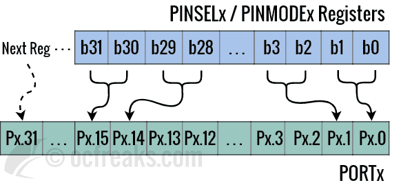

Here ‘bx’ refers to xth Bit and ‘Px.y’ refers to yth Pin on port ‘x’. Just remember that assigning ‘0’ to the corresponding PINSEL registers forces the corresponding pins to be used as GPIO. Since by default all pins are configured as GPIOs we don’t need to explicitly assign a ‘0’ value to PINSEL register in our programming examples.
As per the CMSIS convention, the registers that we saw are grouped into structures. LPC_GPIOx is defined as a pointer to this structure in LPC17xx.h header. These registers are defined as members of this structure. Hence to use any register, for e.g. FIODIR, we must use the arrow “->” operator to de-reference members of structure (since the structure itself is a pointer) to access the register as follows : LPC_GPIO0->FIODIR = some value.
Pins on LPC176x are 5V tolerant when used for GPIO but when used as inputs for ADC block they are not. However, I would recommend that wherever possible, use a buffer for level translation between 5V and 3.3V. If you need any help regarding level translation just let me know in the you comment below.
GPIO Programming & Examples
Now lets see how we can assign values to registers. We can use Hexadecimal notation & decimal notation for assigning values. If your compiler supports other notations like binary notation use can use that too.
Lets say we want to set PIN 3 on Port 0 as output. It can be done in following ways:
CASE 1. LPC_GPIO0->FIODIR = (1<<3); //(binary using left shift - direct assign: other pins set to 0)

CASE 2. LPC_GPIO0->FIODIR |= 0x0000008; // or 0x8; (hexadecimal - OR and assign: other pins not affected)

CASE 3. LPC_GPIO0->FIODIR |= (1<<3); //(binary using left shift - OR and assign: other pins not affected)
- In many scenarios, Case 1 must be avoided since we are directly assigning a value to the register. So while we are making P0.2 ‘1’ others are forced to be assigned a ‘0’ which can be avoided by ORing and then assigning Value.
- Case 2 can be used when bits need to be changed in bulk and
- Case 3 when some or single bit needs to be changed.
First thing to note here is that preceding Zeros in Hexadecimal Notation can be ignored because they have no meaning since we are working with unsigned values here (positive only) which are assigned to Registers. For eg. 0x2F and 0x02F and 0x002F all mean the same.
Finally, All GPIO pins are configured as Input with pullup after Reset by default!
Now, Lets go through some examples :
Example #1)
Consider that we want to configure Pin 4 of Port 0 i.e P0.4 as Ouput and want to drive it High(Logic 1). This can be done as :
LPC_GPIO0->FIODIR |= (1<<4); // Config P0.4 as Ouput
LPC_GPIO0->FIOSET |= (1<<4); // Make ouput High for P0.4
Example #2)
Making output configured Pin 17 High of Port 0 i.e P0.17 and then Low can be does as follows:
LPC_GPIO0->FIODIR |= (1<<17); // P0.17 is Output pin
LPC_GPIO0->FIOSET |= (1<<17); // Output for P0.17 becomes High
LPC_GPIO0->FIOCLR |= (1<<17); // Output for P0.17 becomes Low
Example #3)
Configuring P0.5 and P0.11 as Ouput and Setting them High:
LPC_GPIO0->FIODIR |= (1<<5) | (1<<11); // Config P0.5 and P0.11 as Ouput
LPC_GPIO0->FIOSET |= (1<<5) | (1<<11); // Make ouput High for P0.5 and P0.11
Example #4)
Configuring 1st 8 Pins of Port 0 (P0.0 to P0.7) as Ouput and Setting them High:
LPC_GPIO0->FIODIR |= 0xFF; // Config P0.0 to P0.7 as Ouput
LPC_GPIO0->FIOSET |= 0xFF; // Make output High for P0.0 to P0.7
Now lets play with some real world examples.
Example #5)
Simple Blinky Example - Here we repeatedly make pins 0 to 3 in port 0 (P0.0 to P0.3) High then Low then High and so on. You can connect LED to any 1 pin using 330Ohm series resistor or connect LEDs to all Pins using a buffer ICs like 74HC245 to drive the LEDs. The LED(s) are to be connected between output and ground. Here we will introduce some delay between making all pins High and Low so it can be noticed.
#include <lpc17xx.h>

void delay(void);

int main(void)
{
	LPC_GPIO0->FIODIR = 0xF; // Configure pins 0 to 3 on Port 0 as Output

	while(1)
	{
		LPC_GPIO0->FIOSET = 0xF; // Output HIGH
		delay();
		LPC_GPIO0->FIOCLR = 0xF; // Output LOW
		delay();
	}
	return 0; // normally this wont execute
}

void delay(void) //Hardcoded delay function
{
	int count,i=0;
	for(count=0; count < 6000000; count++) // You can edit this as per your needs
	{
		i++; // something needs to be here else compiler will remove the for loop!
	}
}
Example #6)
Configuring P0.5 as Input and monitoring it for a external event like connecting it to LOW or GND. P0.8 is configured as output and connected to LED. If Input for P0.5 is a 'Low' (GND) then output for P0.8 is made High which will activate the LED and make it glow (Since the other END of LED is connected to LOW i.e GND). Since by default, internal Pull-ups are enabled the 'default' state of the pins configured as Input will be always 'High' unless it is explicitly pulled 'Low' by connecting it to Ground. Consider one end of a tactile switch connected to P0.5 and other to ground. When the switch is pressed a 'LOW' will be applied to P0.5. The setup is shown in the figure below:


#include <lpc17xx.h>

int main(void)
{
	LPC_GPIO0->FIODIR &= ~((1<<5)) ; // explicitly making P0.5 as Input - even though by default its already Input
	LPC_GPIO0->FIODIR |= (1<<8); // Configuring P0.8 as Output

	while(1)
	{
		if( !(LPC_GPIO0->FIOPIN & (1<<5)) ) // Evaluates to True for a 'LOW' on P0.5
		{
			LPC_GPIO0->FIOSET |= (1<<8); // drive P0.8 High
		}
	}
	return 0; // this wont execute normally
}
Example #7)
Now lets extended example 6 so that when the button is pressed, the LED will glow and when released or not pressed the LED won't glow. Capturing inputs in this way, using switches, leads to a phenomenon called 'bouncing' which needs to be resolved using 'debouncing' which I have explained in a previous GPIO tutorial for LPC2100 MCUs - please refer it for explanation. The algorithm used below is very basic for the sake of brevity, you can find a proper debouncing algorithms online.
#include <lpc17xx.h>

void tinyDelay(void);

int main(void)
{
	int flag=0, pinSamplePrev, pinSampleCurr;
	LPC_GPIO0->FIODIR &= ~((1<<5));
	LPC_GPIO0->FIODIR |= (1<<8);

	pinSamplePrev = LPC_GPIO0->FIOPIN & (1<<5); //Initial Sample

	while(1)
	{
		pinSampleCurr = LPC_GPIO0->FIOPIN & (1<<5); //New Sample

		if( pinSampleCurr != pinSamplePrev )
		{
			//P0.5 might get low or high momentarily due to noise depending the external conditions or some other reason
			//hence we again take a sample to insure its not due to noise

			tinyDelay(); // momentary delay

			// now we again read current status of P0.5 from IO0PIN
			pinSampleCurr = LPC_GPIO0->FIOPIN & (1<<5);

			if( pinSampleCurr != pinSamplePrev )
			{
				//State of P0.5 has indeed changed
				if(flag) //First time Flag will be = 0 hence else part will execute
				{
					LPC_GPIO0->FIOSET |= (1<<8); // drive P0.8 High, so LED turns on
					flag=0; //next time 'else' part will excute
				}
				else
				{
					LPC_GPIO0->FIOCLR |= (1<<8); // drive P0.8 Low, so LED turns off
					flag=1; //next time 'if' part will excute
				}

				//set current value as previous since it has been processed
				pinSamplePrev = pinSampleCurr;
			}
		}
	}
	return 0; // this wont execute ever, you can comment it to shut up the compiler complaining.
}

void tinyDelay(void) //Hardcoded delay - use can use timer to get precise delays
{
	int z,c;
	c=0;
	for(z=0; z<3000; z++) //Higher value for higher clock speed
	{
		c++; //just so compiler doesn't remove the 'for' loop
	}
}
Easing play with Bits
Using the left shift operation is not confusing but when too many are used together I find it a little bit messy and affects code readability to some extent. For this I define a Macro BIT(x) as:
#define BIT(x) (1<<x)
After that is defined we can directly use BIT(x). Using this, Example 3 can be re-written as:
LPC_GPIO0->FIODIR |= BIT(5) | BIT(11); // Config P0.4 and P0.21 as Ouput
LPC_GPIO0->FIOSET |= BIT(5) | BIT(11); // Make ouput High for P0.4 and P0.21
Example 6 can be re-written as:
#include <lpc17xx.h>

#define BIT(x) (1<<x)

int main(void)
{
	LPC_GPIO0->FIODIR &= ~(BIT(5));
	LPC_GPIO0->FIODIR |= BIT(8);

	while(1)
	{
		if( !( LPC_GPIO0->FIOPIN & BIT(5) ) )
		{
			LPC_GPIO0->FIOSET |= BIT(8);
		}
	}
	return 0;
}
Similarly, we can define BITN(x) as follow:
#define BITN(x) (!(1<<x))
This gives you 1's complement or Negation for (1<<x). Here xth bit will be 0 and all other bits will be 1s.
Pin modes of Port pins in Cortex-M3 LPC176x MCUs
LPC1768 MCU supports 4 pin modes. These include the internal (on-chip) pull-up and pull-down resistor modes and a special operating mode. Pull-up and Pull-down resistors prevent the inputs from 'floating' by either pulling them to logic HIGH or LOW. The state of the inputs is therefore always defined.
The PINMODE and PINMODE_OD registers together are used to control the pin mode. A total of 3 bits are used to control the mode of a any pin, 2 bits from PINMODE and 1 bit from PINMODE_OD register. Hence we have a total of 10 PINMODE registers and a total of 5 PINMODE_OD. For the pins which are not available the corresponding bits are reserved. Bits 0 & 1 of PINMODE0 corresponds to Pin 0 of Port 0, bits 2 & 3 of PINMODE0 corresponds to Pin 1 of Port 0 and so on. PINMODE_ODx has 1:1 correspondence to all the pins in PORTx.
Pin mode select register bits for PINMODE0-9:
| 00 | Internal pull-up resistor enabled. |
| 01 | Repeater mode - Retains its last state if it is configured as an input and is not driven externally. |
| 10 | Both pull-up and pull-down resistors disabled. |
| 11 | Internal pull-down resistor enabled. |
The PINMODE_OD register controls the open drain mode for port pins. Setting any bit to 1 will enable open-drain mode for the corresponding pin. Setting any bit to 0 will enable the normal(default) mode for the pin.
As a beginner you will be mostly using either Pull-up or Pull-down mode with non open-drain mode (default). You can read more about the Pin Modes on Page 103 of the LPC176x User Manual(Rev. 01).