
When getting started in embedded programming, GPIO (viz. General Purpose Input Output) pins are one of the first things played with. Its also quite evident that the most popular “hello world” program in embedded systems programming is Blinky i.e a LED connected to pin on the Microcontroller that keeps blinking. The use of GPIO is not limited to driving LEDS but can be also used for reading digital signal , generating triggers for external components , controlling external devices and what not. In this tutorial we see how to use and program GPIO Pins for lpc214x ARM 7 microcontrollers from NXP/Philips.
Before getting into this you need to have basic understanding of Binary and Hexadecimal system and Bitwise operations in C.
- Guide to Binary and Hexadecimal system is @ Hexadecimal and Binary Number System basics for Embedded Programming
- Tutorial for Bitwise Operations in C is @ Tutorial : Embedded programming basics in C – bitwise operations
I’ll use ARM7 lpc2148 MCU for explanation and programming examples. The Programs and Register names that I have shown are used in KEIL as defined in lpc214x header file. You can download KEIL UV4 from here. If you are using a different IDE/Compiler then you’ll might need to change the Register Names if required. Also do note that Integer Data-Type i.e. an ‘int’ is always 32 bits in KEIL (i.e the ARM Compiler which it uses) in case of 32bits ARM MCUs like lpc2148 and others.
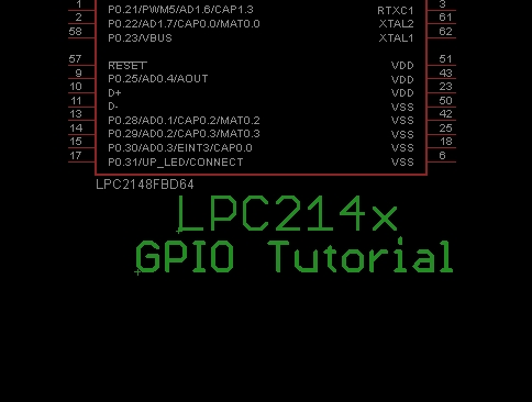
Most of the function oriented pins on lpc214x Microcontrollers are grouped into ports. lpc2148 has 2 ports viz. Port 0 and Port 1.
- Port 0 is a 32 bit wide I/O port (i.e it can be used for max 32 pins where each pin refers to a corresponding bit) and has dedicated direction bits for each of the pins present in the port. 28 out of the 32 pins can be used as bi-directional I/O (digital) pins. Pins P0.24 , P0.26 & P0.27 are unavailable for use and Pin P0.30 can be used as output pin only.
- Port 1 is also a 32 bit wide I/0 port but Pins 0 to 15 i.e P1.0 – P1.15 are unavailable for use and this port too has a dedicated direction bit for each of the usable pins.
In lpc214x MCUs most of the PINS are Multiplexed i.e. these pins can be configured to provide different functions. I’ll explain this in upcoming tutorial. For now Just keep in mind that by default : all functional pins i.e pins in port 0 & 1 are set as GPIO so we can directly use them when learning GPIO usage.
Now , lets go through the registers used for GPIO programming.
2. IOxDIR : This is the GPIO direction control register. Setting a bit to 0 in this register will configure the corresponding pin to be used as an Input while setting it to 1 will configure it as Output.
3. IOxSET : This register can be used to drive an ‘output’ configured pin to Logic 1 i.e HIGH. Writing Zero does NOT have any effect and hence it cannot be used to drive a pin to Logic 0 i.e LOW. For driving pins LOW IOxCLR is used which is explained below.
4. IOxCLR : This register can be used to drive an ‘output’ configured pin to Logic 0 i.e LOW. Writing Zero does NOT have any effect and hence it cannot be used to drive a pin to Logic 1.
Registers Names defined in ‘lpc214x.h’ header file are basically pointers which point to actual register in Hardware. Since lpc214x MCUs are 32 bit , the size of the pointer is also 32 bits. Each bit in these registers mentioned above is directly linked to a corresponding Pin. Manipulating these bits changes the behavior or state of the pins. For e.g consider IOxDIR register. Bit 0 of IO0DIR corresponds to pin 0 of port 0 hence bit ‘y’ in IOxDIR corresponds to pin ‘y’ in port ‘x’.
Now setting PIN 2 of Port 0 i.e P0.2 as output can be done in various ways as show :
CASE 1. IO0DIR = (1<<2);//(binary - direct assign: other pins set to 0)

CASE 2. IO0DIR |= 0x0000004;// or 0x4; (hexadecimal - OR and assign: other pins not affected)

CASE 3. IO0DIR |= (1<<2); //(binary - OR and assign: other pins not affected)
First thing is to note that is preceding Zeros in Hexadecimal Notation can be ignored because they have no meaning since we are working with unsigned values here (positive only) which are assigned to Registers. For eg. ‘0x32’ and ‘0x032’ and ‘0x0032’ all mean the same.
Also note that the BIT and PIN Numbers are Zero(0) indexed which is quite evident since Bit ‘x’ refers to (x-1)th location in the corresponding register.
Case 1 must be avoided since we are directly assigning a value to the register. So while we are making P0.2 ‘1’ others are forced to be assigned a ‘0’ which can be avoided by ORing and then assigning Value.
Case 2 can be used when bits need to be changed in bulk and
Case 3 when some or single bit needs to be changed.
Also Note: All GPIO pins are configured as Input after Reset by default!
Example #1)
Consider that we want to configure Pin 19 of Port 0 i.e P0.19 as Ouput and want to drive it High(Logic 1). This can be done as :
IO0DIR |= (1<<19); // Config P0.19 as Ouput
IO0SET |= (1<<19); // Make ouput High for P0.19
Example #2)
Making output configured Pin 15 High of Port 0 i.e P0.15 and then Low can be does as follows:
IO0DIR |= (1<<15); // P0.15 is Output pin
IO0SET |= (1<<15); // Output for P0.15 becomes High
IO0CLR |= (1<<15); // Output for P0.15 becomes Low
Example #3)
Configuring P0.13 and P0.19 as Ouput and Setting them High:
IO0DIR |= (1<<13) | (1<<19); // Config P0.13 and P0.19 as Ouput
IO0SET |= (1<<13) | (1<<19); // Make ouput High for P0.13 and P0.19
Example #4)
Configuring 1st 16 Pins of Port 0 (P0.0 to P0.15) as Ouput and Setting them High:
IO0DIR |= 0xFFFF; // Config P0.0 to P0.15 as Ouput
IO0SET |= 0xFFFF; // Make ouput High for P0.0 to P0.15
Now lets play with some real world examples.
Example #5)
Blinky Example - Now we repeatedly make first four pins in port 0 (P0.0 to P0.3) High then Low then High and so on. You can connect Led to any one of Pins used. Here we will introduce "hard-coded" delay between making the pins High and Low, so it can be noticed.
#include <lpc214x.h>

void delay(void);

int main(void)
{
	IO0DIR = 0xF; // Configure pins(0 to 3) on Port 0 as Output

	while(1)
	{
		IO0SET = 0xF; // Turn on LEDs
		delay();
		IO0CLR = 0xF; // Turn them off
		delay();
	}
	return 0; // normally this wont execute
}

void delay(void)
{
	int z,c;
	c=0;
	for(z=0; z<4000000; z++) // You can edit this as per your needs
	{
		c++; // something needs to be here else KEIL ARM compiler will remove the for loop!
	}
}
Example #6)
Configuring P0.7 as Input and monitoring it for a external event like connecting it to LOW or GND. P0.30 is configured as output and connected to LED. If Input for P0.7 is a 'Low' (GND) then output for P0.30 is made High which will activate the LED and make it glow (Since the other END of LED is connected to LOW i.e GND). Since internal Pull-ups are enabled the 'default' state of the pins configured as Input will be always 'High' unless it is explicitly made 'Low' by connecting it to Ground. Consider one end of a tactile switch connected to P0.7 and other to ground. When the switch is pressed a 'LOW' will be applied to P0.7. The setup is shown in the figure below:


#include <lpc214x.h>

int main(void)
{
	IO0DIR &= ~((1<<7)) ; // explicitly making P0.7 as Input - even though by default its already Input
	IO0DIR |= (1<<30); // Configuring P0.30 as Output

	while(1)
	{
		if( !(IO0PIN & (1<<7)) ) // Evaluates to True for a 'LOW' on P0.7
		{
			IO0SET |= (1<<30); // drive P0.30 High
		}
	}
	return 0; // this wont execute ever :P
}
'(1<<7)' is simply 7th bit '1'(i.e 0x00000080) & rest all bit are zeros. When '(1<<7)' is ANDed with IO0SET it will make all other bits except 7th bit to '0'. The Value of 7th bit in result will now depend on IO0PIN's 7th bit. If its 1 (which means input is High) then result after ANDing will be 0x00000080 which is greater than zero and hence will evaluate to 'TRUE'. Also when we use 'Logical NOT' i.e '!' then '!(TRUE)' evaluates to FALSE hence code is not executed for High Input. When P0.7 is given 'Low' the corresponding bit in IO0PIN i.e 7th bit will be set to 0. In this case the result of 'IO0PIN & (1<<7)' will be '0x0' which evaluates to FALSE. Hence '!(FALSE)' evalutes to TRUE and code inside 'if' block gets executed.
Example #7)
Now we will extended example 6 so that when the button is pressed the LED will glow and when released or not pressed the LED wont glow. Capturing inputs in this manner, using switches, leads to a phenomenon called 'bouncing' which needs to be resolved using 'debouncing' as explained below.
Bouncing:
Usually in switches there are Metal contacts which Open and Close. Consider an Open switch. When it is closed the signal passes over initially and then briefly the contacts might loosen and possibly result in a Open-Circuit momentarily hence signal doesn't pass over for that short period of time. After this the contacts settle and signal passes over again 'steadily'. This tendency of the metal contacts is referred to as 'Bouncing'.
Debouncing:
Bouncing needs to be given special attention while processing/capturing inputs. Bouncing can be eliminated using 'Debouncing'. Debouncing can be tackled at hardware or software level. In hardware it can be done using RC circuits , Latches , etc.. For the sake of this article I'll show how to deal with it using software. In this we will sample(read) P0.7 status/state two times with a very brief delay in between. In our case this simple strategy is sufficient to prevent bouncing. Note that delay must be correctly chosen - it must not be too high nor too low. If the state of pin is same after taking the second sample then we can say that the new state of the pin is indeed stable.
I would recommend visiting the following links for understanding debouncing in-depth.
1) www.ganssle.com/debouncing.htm
2) www.labbookpages.co.uk/electronics/debounce.html
3) www.eng.uwaterloo.ca/~tnaqvi/downloads/DOC/sd192/SwitchDebouncing.htm
Note: The Example given below is very a crude implementation for debouncing using flags and previous states. It uses hard-coded delays. Proper algorithms are discussed in the links given above.
#include <lpc214x.h>

void tiny_delay(void);

int main(void)
{
	int flag=0, pinSamplePrevious, pinSampleCurrent;
	IO0DIR &= ~((1<<7));
	IO0DIR |= (1<<30);

	pinSamplePrevious = IO0PIN & (1<<7); //Initial Sample

	while(1)
	{
		pinSampleCurrent = IO0PIN & (1<<7); //New Sample

		if( pinSampleCurrent != pinSamplePrevious )
		{
			//P0.7 might get low or high momentarily due to noise depending the external conditions or some other reason
			//hence we again take a sample to insure its not due to noise

			tiny_delay(); // momentary delay

			// now we again read current status of P0.7 from IO0PIN
			pinSampleCurrent = IO0PIN & (1<<7);

			if( pinSampleCurrent != pinSamplePrevious )
			{
				//State of P0.7 has indeed changed
				if(flag) //First time Flag will be = 0 hence else part will execute
				{
					IO0SET |= (1<<30); // drive P0.30 High
					flag=0; //next time 'else' part will excute
				}
				else
				{
					IO0CLR |= (1<<30); // drive P0.30 Low
					flag=1; //next time 'if' part will excute
				}

				//set current value as previous since it has been processed
				pinSamplePrevious = pinSampleCurrent;
			}
		}
	}
	return 0; // this wont execute ever :P
}

void tiny_delay(void)
{
	int z,c;
	c=0;
	for(z=0; z<1500; z++) //Higher value for higher clock speed
	{
		c++;
	}
}
Initially P0.7 will be high since pull-ups are enabled. Hence 'pinSamplePrevious' and 'pinSampleCurrent' will have same value and 'if' will evalute to false so code inside wont execute.
Event #1) Pressing switch: When switch is pressed P0.7 will now be 'Low' but this might be due to noise or glicthy contact in switch so we again read the value of P0.7 to confirm that the new state of P0.7 is stable. If it is stable then value of 'pinSampleCurrent' will differ from 'pinSamplePrevious' and the inner 'if' block evalute to true and code inside will execute. When its executed first time 'flag' will be 0. Hence, 'if(flag)' will be false and 'else' block will execute which will drive P0.30 Low and set flag to '1'.
Event #2) Releasing switch: Now After the switch has been released the value of P0.7 will change to '1' i.e High. Previous state was 'Low' and current is 'High' hence pinSamplePrevious' and 'pinSampleCurrent' will again differ and in similar manner as above the code inside inner 'if' block will execute. This time though , since flag is 1, 'if(flag)' will evaluate to true and P0.30 will be set to High i.e '1' and flag will be set to 0.
Improvising play with Bits:
Using the left shift operation is not confusing but when too many are used together I find it a little bit out of order and affects code readability to some extent. For this I define a Macro 'BIT(x)' which replaces '(1<<x)' as:
#define BIT(x) (1<<x) After that is defined we can directly use BIT(x). Using this Example 3 can be re-written as:
IO0DIR |= BIT(13) | BIT(19); // Config P0.13 and P0.19 as Ouput
IO0SET |= BIT(13) | BIT(19); // Make ouput High for P0.13 and P0.19
Example 6 can be re-written as:
#include <lpc214x.h>

#define BIT(x) (1<<x)

int main(void)
{
	IO0DIR &= ~(BIT(7));
	IO0DIR |= BIT(31);

	while(1)
	{
		if( !(IO0PIN & BIT(7)) )
		{
			IO0SET |= BIT(31);
		}
	}
	return 0;
}
LPC2148 Development Boards that we Recommend:


