basing on a cut down GK110 core on which its big brother runs the GTX 780 is a replacement for its predecessor the GTX 680. It’s the result of Nvidia’s annual refreshment plans which generally translates into :adding more functional units. For a more clear view refer to the chart below.
| GTX TITAN | GTX 780 | GTX 680 | GTX 580 | |
|---|---|---|---|---|
| Stream Processors | 2688 | 2304 | 1536 | 512 |
| Texture Units | 224 | 192 | 128 | 64 |
| ROP | 48 | 48 | 32 | 48 |
| Core Clock | 837Mhz | 863MHz | 1006MHz | 722MHz |
| Shader Clock | N/A | N/A | N/A | 1544MHz |
| Boost Clock | 876MHz | 900MHz | 1058MHz | N/A |
| Memory Clock | 6GHz DDR5 | 6GHz DDR5 | 6GHz DDR5 | 4GHz DDR5 |
| Memory Bus Width | 384-bit | 384-bit | 256-bit | 384-bit |
| VRAM | 6 GB | 3 GB | 2 GB | 1.5 GB |
| FP64 | 1/3 | 1/24 | 1/24 | 1/8 |
| TDP | 250W | 250W | 195W | 244W |
| Transistor Count | 7.1B | 7.1B | 3.5B | 3B |
| Manufacturing Process | 28Nm | 28Nm | 28Nm | 40Nm |
So we can clearly see the GTX 780 is a cut down version of the TITAN for gaming purpose. On the architectural side we’re looking at the same GK110 GPU, this time with fewer functional units like Titan’s 14 SMXes reduced to just 12 SMXes, shaders reduced from 2688 to 2304, and the texture unit count from 224 to 192.
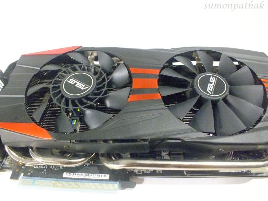
Now with that aside lets see what we have in our hands today.
| Specifications | |
|---|---|
| Model | GTX780-DC2OC-3GD5 |
| Graphics Engine | NVIDIA GeForce GTX 780 |
| Bus Standard | PCI Express 3.0 |
| Video Memory | GDDR5 3GB |
| GPU Boost Clock | 941 MHz |
| GPU Base Clock | 889 MHz |
| CUDA Core | 2304 |
| Memory Clock | 6008 MHz |
| Memory Interface | 384 bit |
| DVI Max. Resolution | 2560 * 1600 |
| DVI Resolution | 1 x Native DVI-I |
| 1 x Native DVI-D | |
| HDMI Output | 1 x Native |
| DisplayPort | 1 x Native |
| HDCP Compliant | YES |
| Dimensions | 11.3×5.8×1.6 Inch |

Now with that aside its time for a little photo shoot.
