
Introduction
In this tutorial we will go through ARM7 processor based LPC2148 ADC programming. Analog to Digital Conversion(i.e. ADC) , as the name suggests , is all about converting a given analog signal into its digital form or say a digital value. So, what does this mean? Well, basically its measuring the voltage of a given analog signal. The analog signal can be differential, single-ended unipolar, etc. The converted digital value represents the measured voltage. This conversion or measurement happens in presence of a fixed and accurate reference voltage. The analog signal is compared to this reference voltage and then estimations are made to get the final measured value. Note that, here the accuracy depends on how accurate the reference voltage is along with ADC’s internal architecture. ADCs come in many varieties, some of these are : Flash ADC , Sigma-Delta (SD) ADC , Successive Approximation (SAR) ADC , etc. There are many application for ADC like Sensor Interfacing, Voltage measurement, Current measurement using shunt , Converting an audio input to its digital form, etc.
Analog to Digital Convertor Block in LPC214x
ADC on LPC214x is based on Successive Approximation(SAR) conversion technique. You can check the wikipedia article on SAR here.
Here are the features of ADC module in ARM7 LPC214x :
- 10 bit SAR ADC (1 in lpc2141/2 and 2 in lpc2144/6/8)
- Supports Power down mode
- Measurement range is from 0 volts to Vref (Reference Voltage)
- 10 bit conversion time is >= 2us
- 6(AD0) & 8(AD1) Multiplexed input pins
- Burst conversion support for Single or Multiple input
Pins relating to ADC Module of LPC214x :
| Pin | Description |
|---|---|
| AD0.1 to AD0.4 (P0.28/29/30/25) and AD0.6, AD0.7 (P0.4/5) | Analog input pins. Note from Datasheet: “If ADC is used, signal levels on analog input pins must not be above the level of Vdda at any time. Otherwise, A/D converter readings will be invalid. If the A/D converter is not used in an application then the pins associated with A/D inputs can be used as 5V tolerant digital IO pins.” |
| Vref | This is the reference voltage pin. It must be connected to an accurate reference voltage source. |
| Vdda, Vssa | Vdda is Analog Power pin and Vssa is Ground pin used to power the ADC module. |
Registers used for ADC programming in LPC214x
(For AD1 registers replace 0 with 1 wherever applicable)
- Bits[7 to 0] – SEL : This group of bits are used to select the pins(Channels) which will be used for sampling and conversion. Bit ‘x'(in this group) is used to select pin A0.x in case of AD0.
- Bits[15 to 8] – CLKDIV : These bits stores the value for CLKDIV which is used to generate the ADC clock. Peripheral clock i.e. PCLK is divided by CLKDIV+1 to get the ADC clock. Note that ADC clock speed must be <= 4.5Mhz! As per datasheet user must program the smallest value in this field which yields a clock speed of 4.5 MHz or a bit less.
- Bit 16 – BURST : Set this to 1 for doing repeated conversions. Set this bit to 0 for software controlled conversions , which take 11 clocks to finish. Here is a remark from datasheet : START bits must be set to 000 when BURST=1 or conversions will not start. Refer datasheet for detailed info.
- Bits[19 to 17] – CLKS : These bits are used to select the number of clocks used for conversion in burst mode along with number of bits of accuracy of the result in RESULT bits of ADDR.
Value clocks / bits 000 11 clocks / 10 bits 001 10 clock / 9 bits 010 9 clock / 8 bits 011 8 clock / 7 bits 100 7 clock / 6 bits 101 6 clock / 5 bits 110 5 clock / 4 bits 111 4 clock / 3 bits - Bit 21 – PDN : Set it to 1 for powering up the ADC and making it operational. Set it to 0 for bringing it in powerdown mode.
- Bits[26 to 24] – START : These bits are used to control the start of ADC conversion when BURST (bit 16) is set to 0. Below is the table as given in datasheet :
Value Significance 000 No start (this value is to be used when clearing PDN to 0) 001 Start the conversion 010 Start conversion when the edge selected by bit 27 occurs on P0.16/EINT0/MAT0.2/CAP0.2 pin 011 Similar to above – for MAT0.0 pin 100 Similar to above – for MAT0.1 pin 101 Similar to above – for MAT0.3 pin 110 Similar to above – for MAT1.0 pin 111 Similar to above – for MAT1.1 pin - Bit 27 – EDGE : Set this bit to 1 to start the conversion on falling edge of the selected CAP/MAT signal and set this bit to 0 to start the conversion on rising edge of the selected signal. (Note: This bit is of used only in the case when the START contains a value between 010 to 111 as shown above.)
- Other bits are reserved.
2) AD0GDR – A/D Global Data Register : This is the global data register for the corresponding ADC module. It contains the ADC’s DONE bit and the result of the most recent A/D conversion.
- Bits[15 to 6] – RESULT : Given DONE(below) is set to 1 these bits give a binary fraction which represents the voltage on the pin selected by the SEL field, divided by the voltage on Vref pin i.e. =V/Vref. A value of zero indicates that voltage on the given pin was less than , equal to or greater than Vssa. And a value of 0x3FF means that the voltage on the given pin was close to, equal to or greater than the reference voltage.
- Bits[26 to 24] – CHN : It gives the channel from which RESULT bits were converted. 000 for channel 0 , 001 for channel 1 and so on.
- Bit 30 – OVERRUN : In burst mode this bit is 1 in case of an Overrun i.e. the result of previous conversion being lost(overwritten). This bit will be cleared after reading AD0GDR.
- Bit 31 – DONE : When ADC conversion completes this bit is 1. When this register(AD0GDR) is read and AD0CR is written, this bit gets cleared i.e. set to 0. If AD0CR is written while a conversion is in progress then this bit is set and a new conversion is started.
- Other bits are reserved.
3) ADGSR – A/D Global Start Register : This register is used to simultaneously start conversion process of both ADC modules.
- Bit 16 – BURST : Same as given for AD0CR.
- Bits[26 to 24] – START : Same as given for AD0CR.
- Bits 27 – EDGE : Same as shown for AD0CR.
- Other bits are reserved.
4) AD0STAT – A/D Status register : This register contains DONE and OVERRUN flags for all of the A/D channels along with A/D interrupt flag.
- Bits[7 to 0] – DONE[7 to 0] : Here xth bit mirrors DONEx status flag from the result register for A/D channel x.
- Bits[15 to 8] – OVERRUN[7 to 0] : Even here the xth bit mirrors OVERRUNx status flag from the result register for A/D channel x
- Bit 16 – ADINT : This bit represents the A/D interrupt flag. It is 1 when any of the individual A/D channel DONE flags is asserted and enabled to contribute to the A/D interrupt via the ADINTEN(given below) register.
- Other bits are reserved.
5) AD0INTEN – A/D Interrupt Enable Register : Using this register interrupts can be enabled or disabled for any ADC channels.
- Bits[0 to 8] – ADINTEN[0 to 8] : If xth bit is set to 1 then an interrupt will be generated on completion of A/D conversion on channel x. Similarly if this bit is set to 0 then an interrupt wont be generated.
6) AD0DR0 to AD0DR7 – A/D Data registers : This register contains the result of the most recent conversion completed on the corresponding channel [0 to 7].
- Bit[15 to 6] : Same as given for AD0GDR.
- Bit 30 – OVERRUN : Same as given for AD0GDR.
- Bit 31 – DONE : Same as given for AD0GDR.
- Other bits are reserved.
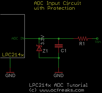
ADC Input circuit and Overvoltage protection
In our case we are going to work with simple Single-ended unipolar signal which varies(or is fixed i.e. DC) between 0V and Vref (Reference voltage). Note that ADC’s cannot measure voltages going above Vref. If a signal goes above Vref then it can lead to an incorrect reading. At the same time we also need to protect the input side of the ADC from over voltage condition. Here is a warning given in LPC214x User Manual:
One of the simplest and neat way to protect the input pins is using a Zener Diode. In our case i.e. in lpc214x overvoltage condition signifies a voltage greater than 3.3Volts. Hence for this we can use a 3.3V zener diode. The datasheet also suggests using a Voltage Source Interface Resistance i.e. Vrsi at the input side with value no more than 40K-Ohms. A typical value of 1.2K ohms can be used which will limit the zener current. In general the value of series resistor depends upon : max zener current, sample and hold capacitor value inside the ADC block and low pass input filter if applicable. If the resistance is too high than the sample and hold capacitor inside SAR ADC of lpc214x will take more time to charge up and we don’t want this to happen. You can also add a 100nF decoupling capacitor if you want to which will form a low pass RC filter. For general ‘DIY project’ purposes, the input circuit schematic is as given below:

Low pass anti-aliasing filter was discussed in LPC214x Sine PWM tutorial under ‘Filter Design’ section which can be found here.
To measure voltages greater than the reference voltage you can use a simply use a voltage divider configuration using 2 resistors with known values. The selection of these resistors depends on the maximum voltage that is to be measured.
LPC214x ADC Modes , Setup and Programming
ADC Operating modes in LPC214x :
1. Software controlled mode : In Software mode only one conversion will be done at a time. This conversion can be controlled in software. To perform another conversion you will need to re-initiate the process. In software mode only 1 bit in the SEL field of AD0CR can be 1 i.e. only 1 Channel(i.e. Pin) can be selected for conversion at a time. You can do conversions on multiple Channels (one at a time) by selecting a particular Channel along with appropriate bit in SEL field and then do the same for rest of the channels.
2. Burst or Hardware mode : In Burst or Hardware mode conversions are performed continuously on the selected channels in round-robin fashion. Since the conversions cannot be controlled by software, Overrun may occur in this mode. Overrun is the case when a previous conversion result is replaced by new conversion result without previous result being read i.e. the conversion is lost. Usually an interrupt is used in Burst mode to get the latest conversion results. This interrupt is triggered when conversion in one of the selected channel ends.
1. Setting up and configuring ADC Module for software controlled mode :
First we will define some values which will help us setup the AD0CR register to configure the AD0 block before we can use it.
#define CLKDIV (15-1) // 4Mhz ADC clock (ADC_CLOCK=PCLK/CLKDIV) where "CLKDIV-1" is actually used , in our case PCLK=60mhz

#define BURST_MODE_OFF (0<<16) // 1 for on and 0 for off

#define PowerUP (1<<21) //setting it to 0 will power it down

#define START_NOW ((0<<26)|(0<<25)|(1<<24)) //001 for starting the conversion immediately

#define ADC_DONE (1<<31)
Here we define CLKDIV which is divided by PCLK to get the ADC clock <=4Mhz. In our case we will be using a PCLK of 60Mhz hence we divide 60Mhz by 15 to get 4Mhz. But note that the ADC module actually needs a value of (CLKDIV-1). This is because it adds "+1" to the value internally (in case if user uses a CLKDIV of 0 it will be still valid). For our purposes CLKDIV is a 'zero-indexed' value hence we must subtract it by 1 before using it. In our case we need to supply a value of 14 i.e. (15-1) to AD0CR. BURST_MODE_OFF(bit 16) , PowerUP(bit 21) and ADC_DONE(bit 31) are defined as required. CLKS_10bit has been defined for 10 bit resolution - you can change the bit combination as per your needs. Finally START_NOW is defined as "001" which is for starting the conversion 'now'. Next we define AD0CR_setup which contains basic configuration for setting up the ADC Module. We feed CLKDIV , BURST_MODE_OFF and PowerUP into AD0CR_setup as follows :
unsigned long AD0CR_setup = (CLKDIV<<8) | BURST_MODE_OFF | PowerUP;
Now we assign AD0CR_setup to AD0CR along with channel selection information to select channels as required. Finally we assign(by ORing) START_NOW to AD0CR to start the conversion process as shown :
AD0CR =  AD0CR_setup | SEL_AD06;
AD0CR |= START_NOW;
Note that AD0CR can be assigned/setup in a single step. But I am doing it in three steps to keep things simpler.
2. Setting up and configuring ADC Module for Burst mode :
Configuring ADC Module is similar to what was done in software controlled mode except here we use the CLKS bits and don't use the START bits in AD0CR. ADC_DONE is also not applicable since we are using an ISR which gets triggered when a conversion completes on any of the enabled channels.
#define CLKDIV (15-1) // 4Mhz ADC clock (ADC_CLOCK=PCLK/CLKDIV) where "CLKDIV-1" is actually used , in our case PCLK=60mhz

#define BURST_MODE_ON (1<<16) // 1 for on and 0 for off

#define CLKS_10bit ((0<<19)|(0<<18)|(0<<17)) //10 bit resolution

#define PowerUP (1<<21) //setting it to 0 will power it down
Here CLKS_10bit is used to select 10 bit ADC resolution. We configure and setup the ADC module in a similar manner(as shown above) as follows :
unsigned int AD0CR_setup = (CLKDIV<<8) | BURST_MODE_ON | CLKS_10bit | PowerUP;
AD0CR =  AD0CR_setup | SEL_AD06 | SEL_AD07;
Note that in this case we can select multiple channels for conversion when setting up AD0CR. START bits are not applicable here since the conversions starts as soon we setup AD0CR register.
3. Fetching the conversion result in software controlled mode :
In software controlled mode we continuously monitor bit 31 in the corresponding channel data register ADDR. If bit 31 changes to 1 from 0 , it means that current conversion has been completed and the result is ready. For example , if we have used channel 6 of AD0 then we monitor for changes in bit 31 as follows :
while( (AD0DR6 & ADC_DONE) == 0 ); //this loop will terminate when bit 31 of AD0DR6 changes to 1.
After this we extract the result which is stored in ADDR bits 6 to 15. Here we right shift ADDR by 6 places and force all other unrelated bits to 0 by using a 10-bit mask value of 0x3FF. 0x3FF is a mask containing 1's in bit locations 0 to 9. In our case with AD0DR6 being used , it can be done as follows :
result = (AD0DR6>>6) & 0x3FF;
4. Fetching the conversion result in Burst mode :
In Burst mode we use an ISR which triggers at the completion of a conversion in any one of the channel. Now , we just need to find the Channel for which the conversion was done. For this we fetch the channel number from AD0GDR which also stores the conversion result. Bits 24 to 26 in AD0GDR contain the channel number. Hence , we shift it 24 places and use a 3bit mask value of 0xF as shown below :
unsigned long AD0GDR_Read = AD0GDR;
int channel = (AD0GDR_Read>>24) & 0xF; //Extract Channel Number
After knowing the Channel number, we have 2 options to fetch the conversion result from. Either we can fetch it from AD0GDR or from AD0DRx of the corresponding channel. In the examples covered in 'examples section' of this tutorial I have used AD0GDR for extracting the conversion result as follows :
int currentResult = (AD0GDR_Read>>6) & 0x3FF; //Extract Conversion Result
ARM7 LPC2148 ADC real world examples
Here is a pic of my setup for testing the given examples(I had used 2x 10KOhms Potentiometer):
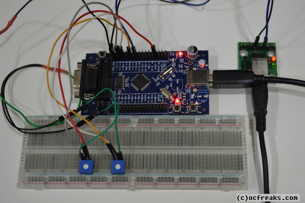

Note that in this case no input protection & filtering was required hence I had skipped it.
ADC Example 1 :
This example uses Software Controlled mode for performing Analog to Digital conversion. In this example we use P0.4 as analog input for measuring the voltage. P0.4 corresponds to Channel 6 of AD0 i.e. AD06. For testing I had used a 10K potentiometer and connected the middle leg to P0.4 of my LPC2148 development board. The connections are as shown below :


Source Code :
/*(C) Umang Gajera - www.ocfreaks.com
More Embedded tutorials @ www.ocfreaks.com/cat/embedded/
LPC2148 ADC Example 1 Source Code.
@ https://www.ocfreaks.com/lpc2148-adc-programming-tutorial/
License : GPL.*/

#include <lpc214x.h>
#include "ocfreaks_sh.h" //OCFreaks LPC214x Tutorial Support Header

#define AD06 ((1<<9)|(1<<8)) //Select AD0.6 function for P0.4
#define SEL_AD06 (1<<6)

#define CLKDIV (15-1) // 4Mhz ADC clock (ADC_CLOCK=PCLK/CLKDIV) where "CLKDIV-1" is actually used , in our case PCLK=60mhz
#define BURST_MODE_OFF (0<<16) // 1 for on and 0 for off
#define PowerUP (1<<21)
#define START_NOW ((0<<26)|(0<<25)|(1<<24)) //001 for starting the conversion immediately
#define ADC_DONE (1<<31)

#define VREF 3.3 //Reference Voltage at VREF pin

int main(void)
{
	initClocks(); //CCLK and PCLK @ 60Mhz - defined in ocfreaks_sh.h
	initUART0(); //Initialize UART0 for printf - defined in ocfreaks_sh.h

	PINSEL0 |= AD06 ; //select AD0.6 for P0.4
	int result=0;
	float voltage = 0;
	unsigned long AD0CR_setup = (CLKDIV<<8) | BURST_MODE_OFF | PowerUP;

	printf("OCFreaks.com ADC Tutorial Example 1.\nSoftware Controlled Mode ADC on AD06 Channel.\n");

	while(1)
	{
		AD0CR =  AD0CR_setup | SEL_AD06;
		AD0CR |= START_NOW; //Start new Conversion

		while( (AD0DR6 & ADC_DONE) == 0 );

		result = (AD0DR6>>6) & 0x3ff;

		voltage = ((float)result*VREF)/1024; //Convert result to volts

		printf("AD06 = %dmV\n" , (int)( voltage*1000 )); //Display millivolts
		delayMS(250); //Slowing down Updates to 4 Updates per second
	}

	//return 0; //This won't execute normally
}
Serial Output :


ADC Example 2 :
This example is similar to Example 1. Here additionally we use P0.5 i.e. AD07 for Analog to Digital Conversion. Even in this case a 10K potentiometer was used for testing. The connections are similar to what given above.
Source Code :
/*(C) Umang Gajera - www.ocfreaks.com
More Embedded tutorials @ www.ocfreaks.com/cat/embedded/
LPC2148 ADC Example 2 Source code.
@ https://www.ocfreaks.com/lpc2148-adc-programming-tutorial/
License : GPL.*/

#include <lpc214x.h>
#include "ocfreaks_sh.h" //OCFreaks LPC214x Tutorial Support Header

#define AD06 ((1<<9)|(1<<8)) //Select AD0.6 function for P0.4
#define AD07 ((1<<11)|(1<<10)) //Select AD0.7 function for P0.5

#define SEL_AD06 (1<<6)
#define SEL_AD07 (1<<7)
#define CLKDIV (15-1) // 4Mhz ADC clock (ADC_CLOCK=PCLK/CLKDIV) where "CLKDIV-1" is actually used , in our case PCLK=60mhz
#define BURST_MODE_OFF (0<<16) // 1 for on and 0 for off
#define PowerUP (1<<21)
#define START_NOW ((0<<26)|(0<<25)|(1<<24)) //001 for starting the conversion immediately
#define ADC_DONE (1<<31)
#define VREF 3.3 //Reference Voltage at VREF Pin

int main(void)
{
	initClocks(); //CCLK and PCLK @ 60Mhz - defined in ocfreaks_sh.h
	initUART0(); //Initialize UART0 for printf - defined in ocfreaks_sh.h

	PINSEL0 |= AD06 | AD07 ; //select AD0.6 and AD0.7 for P0.4 and P0.5
	int result=0;
	float voltage=0;
	unsigned long AD0CR_setup = (CLKDIV<<8) | BURST_MODE_OFF | PowerUP;

	printf("OCFreaks.com ADC Tutorial Example 1.\nSoftware Controlled Mode ADC on AD06 & AD07 Channel.\n");

	while(1)
	{
		//Perform Conversion on Channel 6
		AD0CR =  AD0CR_setup | SEL_AD06;
		AD0CR |= START_NOW; //Start new Conversion
		while( (AD0DR6 & ADC_DONE) == 0 );
		result = (AD0DR6>>6) & 0x3ff;
		voltage = ((float)result*VREF)/1024; //Convert result to volts.
		printf("AD06 = %dmV | " , (int)( voltage*1000 )); //Display millivolts

		//Now Perform Conversion on Channel 7
		AD0CR =  AD0CR_setup | SEL_AD07;
		AD0CR |= START_NOW; //Start new Conversion
		while( (AD0DR7 & ADC_DONE) == 0 );
		result = (AD0DR7>>6) & 0x3ff;
		voltage = ((float)result*VREF)/1024; //Convert result to volts.
		printf("AD07 = %dmV\n" , (int)( voltage*1000 )); //Display millivolts

		delayMS(250); //Slowing down Updates to 4 Updates per second
	}

	//return 0; //this won't execute normally
}
The serial output is similar to example 3 except that this was done in Software mode.
ADC Example 3 :
Here Burst Mode is used for AD conversion. In this example we use an ISR (AD0ISR) which is invoked when a completion occurs in channel 6 or 7. In the ISR we first find the channel number and the extract the result. Here I've used global variables for storing the result so it can be accessed by the 'main()' function which is outside its scope.
Source Code :
/*(C) Umang Gajera - www.ocfreaks.com
More Embedded tutorials @ www.ocfreaks.com/cat/embedded/
LPC2148 ADC Example 3 Source code.
@ https://www.ocfreaks.com/lpc2148-adc-programming-tutorial/
License : GPL.*/

#include <lpc214x.h>
#include "ocfreaks_sh.h" //OCFreaks LPC214x Tutorial Support Header

#define AD06 ((1<<9)|(1<<8)) //Select AD0.6 function for P0.4
#define AD07 ((1<<11)|(1<<10)) //Select AD0.7 function for P0.5

#define ADINTEN6 (1<<6) //Interrupt Enable for Channel 6
#define ADINTEN7 (1<<7) //Interrupt Enable for Channel 7
#define SEL_AD06 (1<<6) //Select Channel 6  for A/D Conversion
#define SEL_AD07 (1<<7) //Select Channel 7 for A/D Conversion

#define CLKDIV (15-1) //4Mhz ADC clock (ADC_CLOCK=PCLK/CLKDIV) where "CLKDIV-1" is actually used , in our case PCLK=60mhz
#define BURST_MODE_ON (1<<16) //1 for on and 0 for off
#define CLKS_10bit ((0<<19)|(0<<18)|(0<<17)) //10bit - used in burst mode only
#define PowerUP (1<<21)
#define VREF 3.3 //Reference Voltage at VREF Pin

void initClocks(void);
void initTimer0(void);
__irq void AD0ISR(void);

void setupPLL0(void);
void feedSeq(void);
void connectPLL0(void);

int AD06Result=0 , AD07Result=0; //Global Variables

int main(void)
{
	initClocks(); //CCLK and PCLK @ 60Mhz - defined in ocfreaks_sh.h
	initUART0(); //Initialize UART0 for printf - defined in ocfreaks_sh.h

	PINSEL0 |= AD06 | AD07 ; //Select AD0.6 and AD0.7 for P0.4 and P0.5 respectively

	VICIntEnable |= (1<<18) ;
	VICVectCntl0 = (1<<5) | 18 ;
	VICVectAddr0 = (unsigned) AD0ISR;

	printf("OCFreaks.com ADC Tutorial Example 3.\nHardware Controlled Mode(BURST Mode) ADC on AD06 & AD07 Channel.\n");

	unsigned long AD0CR_setup = (CLKDIV<<8) | BURST_MODE_ON | CLKS_10bit | PowerUP; //Setup ADC
	AD0INTEN = ADINTEN6 | ADINTEN7 ; //Enable AD06 and AD07 Interrupts
	AD0CR =  AD0CR_setup | SEL_AD06 | SEL_AD07;

	delayMS(10); //Wait till initial conversions get finished

	float volt1=0,volt2=0;

	while(1)
	{
		volt1 = ((float)AD06Result*VREF)/1024; //Convert AD0.6 result to volts.
		volt2 = ((float)AD07Result*VREF)/1024; //Convert AD0.7 result to volts.
		printf("AD06 = %dmV | AD07 = %dmV\n",(int)(volt1*1000),(int)(volt2*1000)); //Display millivolts
		delayMS(250); //4 updates per second
	}

	//return 0; //this wont execute normally
}

__irq void AD0ISR(void) //AD0 Interrupt Function
{
	unsigned long dummyRead;
	unsigned long AD0GDR_Read = AD0GDR;

	int channel = (AD0GDR_Read>>24) & 0xF; //Extract Channel Number
	int currentResult = (AD0GDR_Read>>6) & 0x3FF; //Extract Conversion Result

	if(channel == 6)
	{
		dummyRead = AD0DR6; //Read to Clear Done flag , Also clears AD0 interrupt
		AD06Result = currentResult;
	}
	else if(channel == 7)
	{
		dummyRead = AD0DR7; //Read to Clear Done flag , Also clears AD0 interrupt
		AD07Result = currentResult;
	}

	VICVectAddr = 0x0; //Signal that ISR has finished
}
Serial Output :

