Introduction
This Tutorial is for learning Pulse Width Modulation (PWM) programming for ARM7 based LPC214x MCUs. For this Tutorial I’ll be covering Single Edge PWM and how to use to control Motors like Servos. Also for the scope of this tutorial I won’t be going into stuff like MCU controlled Voltage Regulation using PWM since I am planning a dedicated tutorial for that. I assume you are comfortable with Timers and its usage in LPC214x since PWM block is basically a Timer. I’ve posted a tutorial on Timers in LPC214x @ LPC2148 Timer Tutorial – just in case if you need it.
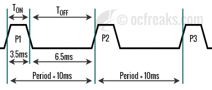
Pulse Width Modulation Basics :
I’ve Posted a Beginner PWM tutorial @ Basic PWM Tutorial. If you are new to PWM please have a look there.
Here is Diagram that sums it up. It shows Single Edge PWM with T-ON , T-OFF & Period. Duty Cycle is simply T-ON Divided by Period.

PWM Programming in ARM7 LPC2148
LPC2148 supports 2 types of PWM :
1) Single Edge PWM – Pulse starts with new Period i.e pulse is always at the beginning
2) Double Edge PWM – Pulse can be anywhere within the Period
A PWM block , like a Timer block , has a Timer Counter and an associated Prescale Register along with Match Registers. These work exactly the same way as in the case of Timers. I’ve explained them in the introduction part of the Lpc214x Timer tutorial @ LPC2148 Timer Tutorial . Match Registers 1 to 6 (except 0) are pinned on LPC214x i.e. the corresponding outputs are diverted to actual Pins on LPC214x MCU. The PWM function must be selected for these Pins to get the PWM output. These pins are :
| Output : | PWM1 | PWM2 | PWM3 | PWM4 | PWM5 | PWM6 |
| Pin Name : | P0.0 | P0.7 | P0.1 | P0.8 | P0.21 | P0.9 |
In LPC214x we have 7 match registers inside the PWM block . Generally the first Match register PWMMR0 is used to generate PWM period and hence we are left with 6 Match Registers PWMMR1 to PWMMR6 to generate 6 Single Edge PWM signals or 3 Double Edge PWM signals. Double edge PWM uses 2 match registers hence we can get only 3 double edge outputs. The way this works in case of Single Edge PWM is as follows (and similarly for Double Edge):
- Consider that our PWM Period duration is 5 milliseconds and TC increments every 1 millisecond using appropriate prescale value.
- Now we set the match value in PWMMR0 as 5 , Note : This period will be same for all PWM outputs!
- Then we configure PWM block such that when TC reaches value in PWMMR0 it is reset and a new Period begins.
- Now lets say we want 2 PWM signals of Pulse widths 2ms and 4ms.
- So .. we can use PWMMR1 and PWMMR2 to get the 2 outputs. For that we set PWMMR1 = 2 and PWMMR2 = 4.
- Then , Everytime a new period starts the Pin corresponding to PWMMR1 and PWMMR2 will be set High by default.
- And .. Whenever the value in TC reaches PWMMR1 and PWMMR2 its output will be set to low respectively.
- Their outputs will remain low until the next Period starts after which their outputs again become high .. hence giving us Single Edge PWM.
This can be shown in the diagram below:


- 1) All single edged PWM outputs will go high at the beginning of a PWM cycle unless their match value is 0.
- 2) Each PWM output will go low when its match value is reached. Note : If no match occurs i.e Match value is greater than Period then the output will remain high!
For Double Edge Rules you can refer the User Manual Pg. 261.
Note 2: Note that Here we are storing the width of the Pulse in the Match Register. We can also change the width of the pulse by changing the value in the corresponding Match register using a special register called Latch Enable Register which is used to control the way Match Registers get updated. I’ll explain this shortly. First Lets see all the Registers in PWM Block in LPC2148.
1) PWMTCR : PWM Timer Control Register
This register is used to control the Timer Counter inside the PWM block. Only Bits: 0, 1 & 3 are used rest are reserverd.
- Bit 0 : This bit is used to Enable/Disable Counting. When 1 both PWM Timer counter and PWM Prescale counter are enabled. When 0 both are disabled.
- Bit 1 : This bit is used to Reset both Timer and Prescale counter inside the PWM block. When set to 1 it will reset both of them (at next edge of PCLK).
- Bit 3 : This is used to enable the PWM mode i.e the PWM outputs.
- Other Bits : Reserved.
2) PWMPR : PWM Prescale Register
PWMPR is used to control the resolution of the PWM outputs. The Timer Counter(TC) will increment every PWMPR+1 Peripheral Clock Cycles (PCLK).
3) PWMMR0 – PWMMR6 : Match Registers
These are the seven Match registers as explained above which contain Pulse Width Values i.e the Number of PWMTC Ticks.
4) PWMMCR : PWM Match Control Registers
The PWM Match Control Register is used to specify what operations can be done when the value in a particular Match register equals the value in TC. For each Match Register we have 3 options : Either generate an Interrupt , or Reset the TC , or Stop .. which stops the counters and disables PWM. Hence this register is divided into group of 3 bits. The first 3 bits are for Match Register 0 i.e PWMMR0 , next 3 for PWMMR1 , and so on :
- 1) Bit 0 : Interrupt on PWMMR0 Match – If set to 1 then it will generate an Interrupt else disable if set to 0.
- 2) Bit 1 : Reset on PWMMR0 Match – If set to 1 it will reset the Timer Counter i.e PWMTC else disabled if set to 0.
- 3) Bit 2 : Stop on PWMMR0 Match – If this bit is set 1 then both PWMTC and PWMPC will be stopped and will also make Bit 0 in PWMTCR to 0 which in turn will disable the Counters.
- *) Similarly {Bits 3,4,5} for PWMMR1 , {Bits 6,7,8} for PWMMR2 , {Bits 9,10,11} for PWMMR3 ,{Bits 12,13,14} for PWMMR4 ,{Bits 15,16,17} for PWMMR5 , {Bits 18,19,20} for PWMMR6.
5) PWMIR : PWM Interrupt Register
If an interrupt is generated by any of the Match Register then the corresponding bit in PWMIR will be set high. Writing a 1 to the corresponding location will clear that interrupt. Here :
- 1) Bits 0,1,2,3 are for PWMMR0, PWMMR1, PWMMR2, PWMMR3 respectively and
- 2) Bits 8,9,10 are for PWMMR4 , PWMMR5 , PWMMR6 respectively. Other bits are reserved.
6) PWMLER : Latch Enable Register
The PWM Latch Enable Register is used to control the way Match Registers are updated when PWM generation is active. When PWM mode is active and we apply new values to the Match Registers the new values won’t get applied immediately. Instead what happens is that the value is written to a “Shadow Register” .. it can be thought of as a duplicate Match Register. Each Match Register has a corresponding Shadow Register. The value in this Shadow Register is transferred to the actual Match Register when :
2) And the corresponding Bit in PWMLER is 1.
Hence only when these 2 conditions are satisfied the value is copied to Match Register. Bit ‘x’ in PWMLER corresponds to match Register ‘x’. I.e Bit 0 is for PWMMR0 , Bit 1 for PWMMR1 , .. and so on. Using PWMLER will be covered in the examples section.
7) PWMPCR : PWM Control Register
This register is used for Selecting between Single Edged & Double Edged outputs and also to Enable/Disable the 6 PWM outputs which go to their corresponding Pins.
- 1) Bits 2 to 6 are used to select between Single or Double Edge mode for PWM 2,3,4,5,6 outputs.
1) Bit 2 : If set to 1 then PWM2(i.e the one corresponding to PWMMR2) output is double edged else if set 0 then its Single Edged.
2) Similarly {Bits 3,4,5,6} for PWM3 , PWM4 , PWM5 , PWM6 respectively. - 2) Bits 9 to 14 are used to Enable/Disable PWM outputs
1) Bit 9 : If set to 1 then PWM1 output is enabled , else disabled if set to 0.
2)Similarly {Bit 10,11,12,13,14} for PWM2 , PWM3 , PWM4 , PWM5 , PWM6 respectively.
Configuring and Initializing PWM:
Configuring PWM is very much similar to Configuring Timer except, additionally, we need to enable the outputs and select PWM functions for the corresponding PIN on which output will be available. But first we need to do some basic Math Calculations for defining the Period time , the resolution using a prescaler value and then Pulse Widths. For this First we need to define the resolution of out PWM signal. Here the PWM resolution which I mean is the minimum increment that can use to increase or decrease the pulse width. More smaller the increment more fine will be the resolution. This resolution is defined using an appropriate Prescale Value. The calculation for Prescale is the same which I had shown in the Timer Tutorial .. but here it is once again :
LPC2148 PWM Prescaler (PWMPR) Calculations:
The delay or time required for ‘Y’ clock cycles of PCLK at ‘X’ MHz is given by :


When we take PR into consideration we get Y = PR+1. Now , consider that PCLK is running at 60Mhz then X=60. Hence if we use Y=60 i.e PR=59 then we get a delay of exact 1 micro-second(s).
So with PR=59 and PCLK @ 60Mhz our formula reduces to :


Similarly when we set Y=60000 i.e PR = 59999 the delay will be 1 milli-second(s) :


This delay which is defined using Prescale will be the delay required for TC to increment by 1 i.e TC will increment every ‘PR+1’ “Peripheral” Clock Cycles (PCLK).
- Select the PWM function for the PIN on which you need the PWM output using PINSEL0/1 register.
- Select Single Edge or Double Edge Mode using PWMPCR. By default its Single Edge Mode.
- Assign the Calculated value to PR.
- Set the Value for PWM Period in PWMMR0.
- Set the Values for other Match Registers i.e the Pulse Widths.
- Set appropriate bit values in PWMMCR .. like for e.g. resetting PWMTC for PWMMR0 match and optionally generate interrupts if required
- Set Latch Enable Bits for the Match Registers that you’ve used. This is important!
- Then Enable PWM outputs using PWMPCR.
- Now Reset PWM Timer using PWMTCR.
- Finally .. Enable Timer Counter and PWM Mode using PWMTCR.
Example :
PINSEL0 = ... ; // Select PWM Function for used Pins
PWMPCR = ... ; // Select PWM type - By default its Single Edged
PWMPR = ... ; //assign calculated PR value
PWMMR0 = ... ; // Assign Period Duration
PWMMRx = ... ; // Assign pulse duration i.e widths for other Match Regs.. x=1 to 6
PWMMCR = (1<<1) | ... ; // Reset PWMTC on PWMMR0 match & Other conditions
PWMLER = (1<<1) | ... ; // update MR0 and other Match Registers
PWMPCR = ... ; // enable PWM outputs as required
PWMTCR = (1<<1) ; //Reset PWM TC & PR

//Now , the final moment - enable everything
PWMTCR = (1<<0) | (1<<3); // enable counters and PWM Mode
//Done!
Updating Match Registers i.e the Pulse Width
Once PWM is initialized then you can update any of the Match Registers at anytime using PWMLER. This can be done as follows :
PWMMR1 = 50; // Update Pulse Width
PWMLER = (1<<1); // set the corresponding bit to 1
When you want to update Multiple Match Registers then this can be done as follows :
PWMMR1 = 50;
PWMMR2 = 68;
PWMMR3 = 20;

PWMLER = (1<<1) | (1<<2) | (1<<3); // Update Latch Enable bit for all MRs together
Some Real World Examples with sample code
I'll cover 2 examples using Single Edge PWM. These will be:
1) Controlling RC Servo
2) LED Dimming
To stay within the scope of this article I'm not including a bit involved stuff like "RC Servo Speed Control" and "DC Motor Speed Control". I guess I'll do it in a separate article.
LPC214x PLL Tutorial for CPU and Peripheral Clock.
Example #1) Simple RC Servo Control Using PWM :
Here we will use PWM1 output from Pin P0.0 to control a RC Servo Motor. We will also be using 4 tactile switches to bring the Servo at 4 different positions. P0.1 , P0.2 , P0.3 , P0.4 will be used to take the input. One end of the tactile switches will be connected to each of these Pins and other end will be connected to ground. Here we'll also require external 5V-6V source to drive the servo. Servos can work with 3.3v voltage levels for input PWM signal , hence we just need to connect the MCU PWM Output to Servo PWM Input wire. The setup is as shown in the schematic below :


When the user will press P0.1 the Pulse width will be 1ms , and similarly when the user presses P0.2 , P0.3 , P0.4 the Pulse Width will change to 1.25ms , 1.5ms and 1.75ms respectively and hence Servo will change its position correspondingly.
Source for Example 1:
/*
(C) Umang Gajera | Power_user_EX - www.ocfreaks.com 2011-13.
More Embedded tutorials @ www.ocfreaks.com/cat/embedded

LPC2148 PWM Tutorial Example 1 - RC Servo Control using PWM.
License : GPL.
*/
#include <lpc214x.h>

#define PLOCK 0x00000400
#define PWMPRESCALE 60   //60 PCLK cycles to increment TC by 1 i.e 1 Micro-second

void initPWM(void);
void initClocks(void);

int main(void)
{
	initClocks(); //Initialize CPU and Peripheral Clocks @ 60Mhz
	initPWM(); //Initialize PWM

    //IO0DIR = 0x1; This is not needed!
    //Also by default all pins are configured as Inputs after MCU Reset.

    while(1)
    {
		if( !((IO0PIN) & (1<<1)) ) // Check P0.1
		{
			PWMMR1 = 1000;
			PWMLER = (1<<1); //Update Latch Enable bit for PWMMR1
		}
		else if( !((IO0PIN) & (1<<2)) ) // Check P0.2
		{
			PWMMR1 = 1250;
			PWMLER = (1<<1);
		}
		else if( !((IO0PIN) & (1<<3)) ) // Check P0.3
		{
			PWMMR1 = 1500;
			PWMLER = (1<<1);
		}
		else if( !((IO0PIN) & (1<<4)) ) // Check P0.4
		{
			PWMMR1 = 1750;
			PWMLER = (1<<1);
		}
    }
    //return 0; //normally this wont execute ever
}

void initPWM(void)
{
	/*Assuming that PLL0 has been setup with CCLK = 60Mhz and PCLK also = 60Mhz.*/
	/*This is a per the Setup & Init Sequence given in the tutorial*/

	PINSEL0 = (1<<1); // Select PWM1 output for Pin0.0
	PWMPCR = 0x0; //Select Single Edge PWM - by default its single Edged so this line can be removed
	PWMPR = PWMPRESCALE-1; // 1 micro-second resolution
	PWMMR0 = 20000; // 20ms = 20k us - period duration
	PWMMR1 = 1000; // 1ms - pulse duration i.e width
	PWMMCR = (1<<1); // Reset PWMTC on PWMMR0 match
	PWMLER = (1<<1) | (1<<0); // update MR0 and MR1
	PWMPCR = (1<<9); // enable PWM output
	PWMTCR = (1<<1) ; //Reset PWM TC & PR

	//Now , the final moment - enable everything
	PWMTCR = (1<<0) | (1<<3); // enable counters and PWM Mode

	//PWM Generation goes active now!!
	//Now you can get the PWM output at Pin P0.0!
}
Example #2) LED Dimming using PWM :
The basic Setup here is same as in Example 1 except that here we replace Servo by a LED and we dont need external 5V source along with slightly modified Program. Here we'll just need to connect the anode of LED to P0.0 and cathode to GND. In this example will use a period of 10ms. In this case the Pulse Widths Corresponding to the Switches connected to P0.1/2/3/4 will be 2.5ms/5ms/7.5ms/10ms respectively. As the Pulse Width Increases LED will keep on getting Brighter and the reverse will happen if Pulse Width is decreased.
Source for Example 2:
/*
(C) Umang Gajera | Power_user_EX - www.ocfreaks.com 2011-13.
More Embedded tutorials @ www.ocfreaks.com/cat/embedded

LPC2148 PWM Tutorial Example 2 - LED Dimming using PWM.
License : GPL.
*/
#include <lpc214x.h>

#define PLOCK 0x00000400
#define PWMPRESCALE 60   //60 PCLK cycles to increment TC by 1 i.e 1 Micro-second

void initPWM(void);
void initClocks(void);

int main(void)
{
	initClocks(); //Initialize CPU and Peripheral Clocks @ 60Mhz
	initPWM(); //Initialize PWM

    //IO0DIR = 0x1; This is not needed!
    //Also by default all pins are configured as Inputs after MCU Reset.

    while(1)
    {
		if( !((IO0PIN) & (1<<1)) ) // Check P0.1
		{
			PWMMR1 = 2500; //T-ON=25% , Hence 25% Bright
			PWMLER = (1<<1); //Update Latch Enable bit for PWMMR1
		}
		else if( !((IO0PIN) & (1<<2)) ) // Check P0.2
		{
			PWMMR1 = 5000; //50% Bright
			PWMLER = (1<<1);
		}
		else if( !((IO0PIN) & (1<<3)) ) // Check P0.3
		{
			PWMMR1 = 7500; //75% Bright
			PWMLER = (1<<1);
		}
		else if( !((IO0PIN) & (1<<4)) ) // Check P0.4
		{
			PWMMR1 = 10000; //100% Bright
			PWMLER = (1<<1);
		}
    }
    //return 0; //normally this wont execute ever
}

void initPWM(void)
{
	/*Assuming that PLL0 has been setup with CCLK = 60Mhz and PCLK also = 60Mhz.*/
	/*This is a per the Setup & Init Sequence given in the tutorial*/

	PINSEL0 = (1<<1); // Select PWM1 output for Pin0.0
	PWMPCR = 0x0; //Select Single Edge PWM - by default its single Edged so this line can be removed
	PWMPR = PWMPRESCALE-1; // 1 micro-second resolution
	PWMMR0 = 10000; // 10ms period duration
	PWMMR1 = 2500; // 2.5ms - pulse duration i.e width (Brigtness level)
	PWMMCR = (1<<1); // Reset PWMTC on PWMMR0 match
	PWMLER = (1<<1) | (1<<0); // update MR0 and MR1
	PWMPCR = (1<<9); // enable PWM output
	PWMTCR = (1<<1) ; //Reset PWM TC & PR

	//Now , the final moment - enable everything
	PWMTCR = (1<<0) | (1<<3); // enable counters and PWM Mode

	//PWM Generation goes active now - LED must be 25% Bright after Reset!!
	//Now you can get the PWM output at Pin P0.0!
}
More stuff using PWM
I've had 2 requests for Sine Wave generation using PWM , which I'll be doing soon which you can find here : Sine Wave Generator using PWM with LPC2148 Microcontroller Tutorial. I might also cover MCU controlled voltage Regulation along with double egde PWM 🙂
Please do leave your Article Requests , Suggestions & Comments.