Hi again guys! In this tutorial we will go through the basics of UART(SERIAL) programming for LPC214x family of microcontrollers. If you are new to UART, you can go through the basic UART tutorial which I’ve posted @ Basic Uart Tutorial.
Introduction
Here is a quick recap of UART basics :
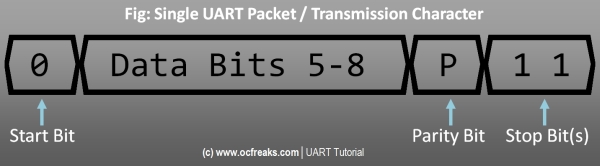
Uart uses TxD(Transmit) Pin for sending Data and RxD(Receive) Pin to get data. UART sends & receives data in form of chunks or packets. These chunks or packets are also referred to as ‘transmission characters’. The structure of a UART data packet is as shown below :

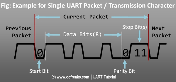
Here is an example of single data packet i.e transmission character :

Now , Lets start with the main Tutorial. LPC214x has 2 UART blocks which are UART0 and UART1. For UART0 the TxD pin is P0.0 and RxD pin is P0.1 and similarly for UART 1 the TxD pin is P0.8 and RxD pin is P0.9 as shown in the table below :
| Pins: | TxD | RxD |
| UART0 | P0.0 | P0.1 |
| UART1 | P0.8 | P0.9 |
Tx has THR(Transmit Holding Register) and TSR(Transmit Shift Register) – When we write Data to be sent into THR it is then transferred to TSR which assembles the data to be transmitted via Tx Pin.
Similarly Rx has RSR(Receive Shift Register) and RBR(Receive Buffer Register) – When a valid data is Received at Rx Pin it is first assembled in RSR and then passed in to Rx FIFO which can be then accessed via RBR.
Registers used for UART programming in LPC214x
Before we can use these pins to transfer data , first we need to configure and initialize the UART block in our LPC214x microcontroller. But before doing that, lets go through some of the important registers: (for UART1 registers replace 0 with 1)
Data Related Registers :
1) U0RBR – Receiver Buffer Register (READ ONLY!): This register contains the top most byte(8-bit data chunk) in the Rx FIFO i.e the oldest received data in FIFO. To properly read data from U0RBR , the DLAB(Divisor Latch Access) bit in U0LCR register must be first set to 0. Also , as per the user manual “The right approach for fetching the valid pair of received byte and its status bits is first to read the content of the U0LSR register, and then to read a byte from the U0RBR.” (Note : If you are using 7,6 or 5 Bits for data then other remaining bits are automatically padded with 0s)
2) U0THR – Transmit Holding Register (WRITE ONLY!): U0THR contains the top most byte in Tx FIFO and in this case its the newest(latest) transmitted data. As in the case with U0RBR , we must set DLAB=0 to access U0THR for write operation.
Baud Rate Setup related registers :
1) U0DLL and U0DLM – Divisor Latch registers: Both of them hold 8-bit values. These register together form a 16-bit divisor value which is used in baud rate generation which we will see in later section. U0DLM holds the upper 8-bits and U0DLL holds the lower 8-bits and the formation is “[U0DLM:U0DLL]“. Since these form a divisor value and division by zero is invalid, the starting value for U0DLL is 0x01 (and not 0x00) i.e the starting value in combined formation is “[0x00:0x01]” i.e 0x0001. Please keep this in mind while doing baud-rate calculations. In order to access and use these registers properly, DLAB bit in U0LCR must be first set to 1.
2) U0FDR – Fractional Divider Register : This register is used to set the prescale value for baud rate generation. The input clock is the peripheral clock and output is the desired clock defined by this register. This register actually holds to different 4-bit values (a divisor and a multiplier) for prescaling which are:
- Bit [3 to 0] – DIVADDVAL : This is the prescale divisor value. If this value if 0 then fractional baud rate generator wont have any effect on Uart Baud rate.
- Bit [7 to 4] – MULVAL : This is prescale multiplier value. Even if fractional baud rate generator is not used the value in this register must be more than or equal to 1 else UART0 will not operate properly.
- Other Bits reserved.
Remark from Usermanual : “If the fractional divider is active (DIVADDVAL > 0) and DLM = 0, the value of the DLL register must be 2 or greater!”
Control and Status Registers :
1) U0FCR – FIFO Control Register : Used to control Rx/Tx FIFO operations.
- Bit 0 – FIFO Enable : 1 to Enable both Rx and Tx FIFOs and 0 to disable.
- Bit 1 – Rx FIFO Reset : Writing a 1 will clear and reset Rx FIFO.
- Bit 2 – Tx FIFO Reset : Writing a 1 will clear and reset Tx FIFO.
- Bits [7 to 6] : Used to determine that how many UART0 Rx FIFO characters must be written before an interrupt is activated.
[00] (i.e trigger level 0) for 1 character.
[01] (i.e trigger level 1) for 4 characters.
[10] (i.e trigger level 2) for 8 characters.
[11] (i.e trigger level 3) for 14 characters. - Others bits are reserved.
2) U0LCR – Line Control Register : Used to configure the UART block (i.e the data format used in transmission).
- Bit [1 to 0] – Word Length Select : Used to select the length of an individual data chunk. [00] for 5 bit character length. Similarly [01] , [10] , [11] for 6 , 7 , 8 bit character lengths respectively.
- Bit 2 – Stop bit select : 0 for using 1 stop bit and 1 for using 2 stop bits.
- Bit 3 – Parity Enable : 0 to disabled Partiy generation & checking and 1 to enable it.
- Bit [5 to 4] – Parity Select : [00] to Odd-parity , [01] for Even-parity , [10] for forced “1”(Mark) parity and [11] for forced “0”(Space) parity.
- Bit 6 – Break Control : 0 to disable break transmission and 1 to enable it. TxD pin will be forced to logic 0 when this bit is 1!
- Bit 7 – Divisior Latch Access bit : 0 to disable access to divisor latches and 1 to enable access.
3) U0LSR – Line Status Register : used to read the status of Rx and Tx blocks.
- Bit 0 – Receiver Data Ready(RDR) : 0 means U0RBR is empty(i.e Rx FIFO is empty) and 1 means U0RBR contains valid data.
- Bit 1 – Overrun Error(OE) : 0 means Overrun hasn’t occured and 1 means Overrun has occured. Overrun is the condition when RSR(Receive Shift Register)[See note 1] has new character assembled but the RBR FIFO is full and the new assembled character is eventually lost since no data is written into FIFO if its full. (Note: Reading U0LSR clears this bit)
- Bit 2 – Parity Error(PE) : 0 mean no parity error and 1 mean a parity error has occured. When the value of the parity bit in the recieved character is in wrong state then a parity error occurs. (Note: Reading U0LSR clears this bit)
- Bit 3 – Framing Error(FE) : 0 means no framing error has occured and 1 means that a framing error has taken place. Framing error occurs when the stop bit of a received character is zero. (Note: Reading U0LSR clears this bit)
- Bit 4 – Break Interrupt : 0 means no Break Interrupt occures and 1 means that it has occured. A Break Interrupt occurs when the RxD line is pulled low (i.e all 0s) i.e held in spacing state for 1 full character after which Rx Block goes into Idle state. Rx Block gets back to active state when RxD pin is pulled high (i.e all 1s) i.e held in marking state for 1 full character. (Note: Reading U0LSR clears this bit)
- Bit 5 – Transmit Holding Register Empty(THRE) : 0 means U0THR contains valid data and 1 means its empty.
- Bit 6 – Transmitter Empty (TEMT) : 0 means U0THR and/or U0RSR contains valid data and 1 means that both U0THR and U0RSR are empty.
- Bit 7 – Error in RX FIFO(RXFE) : 0 means that U0RBR has no Rx Errors or Rx FIFO is disabled(i.e 0th bit in U0FCR is 0) and 1 means that U0RBR has atleast one error. (Note: This bit is cleared only if U0LSR is read and there are no other subsequent errors in Rx FIFO .. else this bit will stay 1)
4) U0TER – Transmit Enable Register : This register is used to enable UART transmission. When bit-7 (i.e TXEN) is set to 1 Tx block will be enabled and will keep on transmitting data as soon as its ready. If bit-7 is set to 0 then Tx will stop transmission. Other bits are reserved.
Interrupt Related Registers :
1) U0IER – Interrupt Enable Register: Set a bit to 0 to disable and 1 to enable the corresponding interrupt.
- Bit 0 – RBR Interrupt Enable
- Bit 1 – THRE Interrupt Enable
- Bit 2 – RX Line Status Interrupt Enable
- Bit 3 – ATBOInt Enable
- Bit 4 – ATEOInt Enable
Where ATBOInt = Auto Baud Time-Out Interrupt , ATEO = End of Auto Baud Interrupt and rest of the bits are reserved.
2) U0IIR – Interrupt Identification Register: Refer User Manual when in doubt. In some application the usage of this register might get a bit complicated.
This register is organized as follows:
- Bit 0 – Interrupt Pending : 0 means atleast one interrupt is pending , 1 means no interrupts are pending. Note: This bit is ACTIVE LOW!
- Bits [3 to 1] – Interrupt Identification : [011] is for Receive Line Status(RLS) , [010] means Receive Data Available(RDA) , 110 is for Character Time-out Indicator(CTI) , [001] is for THRE Interrupt.
- Bits [7 to 6] – FIFO Enable.
- Bit 8 – ABEOInt : 1 means Auto Baud Interrupt has successfully ended and 0 otherwise.
- Bit 9 – ABTOInt : 1 means Auto Baud Interrupt has Timed-out.
- All others bits are reserved.
UART Baud Rate Generation:
The master formula for calculating baud rate is given as :


which can be further simplified to :


with following conditions strictly applied :
0 < MULVAL <= 15
0 <= DIVADDVAL <= 15
if DIVADDVAL > 0 & DLM = 0 then, DLL >= 2
As it can been seen this formula has 2 prominent parts which are : A Base value and a Fractional Multiplier i.e:
This Fractional Multiplier can be used to scale down or keep the base value as it is .. hence its very useful for fine-tuning and getting the baudrate as accurate as possible.
Where PCLK is the Peripheral Clock value in Hz , U0DLM and U0DLL are the divisor registers which we saw earlier and finally DIVADDVAL and MULVAL are part of the Fractional baudrate generator register.
Now we know the formula .. how we do actually start ?
1) The Dirty and Simplest Method:
The quickest and also the dirtiest(accuracy wise) method without using any algorithm or finetuning is to set DLM=0 and completely ignore the fraction by setting it to 1. In this case MULVAL=1 and DIVADDVAL=0 which makes the Fraction Multiplier = 1. Now we are left with only 1 unknown in the equation which is U0DLL and hence we simplify the equation and solve for U0DLL.


But I’d recommend that stay away from above method, if possible, as it works only for particular bauds given a specific PCLK value and moreover U0DLL might get out of range i.e. > 255 in which case you have to start increasing DLM and recompute a new value for U0DLL.
2) The more involved method(Recommended):
Now lets see three examples for calculating Baud Rates Manually using some finetuning :
In these method we again start with DLM=0 , DIVADDVAL=0 and MULVAL=1 and get an initial value for DLM. If you are lucky you will get a very close baudrate to the desired one. If not then we perform some finetuning using DLM , MULVAL and DIVADDVAL and get a new value for DLM. There is on one single method to perform finetuning and one can also make an algorithm for computing the best match given the desired baudrate and PCLK. The finetuning method which I have given below is a basic one suitable for beginners(in my opinion :P).
Ex 1 : PCLK = 30 Mhz and Required Baud Rate is 9600 bauds.
Lets start with U0DLM = 0 , DIVADDVAL = 0 and MULVAL = 1
We have PCLK = 30 Mhz = 30 x 106 Hz
So the equation now gets simplified and we can find U0DLL.
We get U0DLL = 195.3125 , since it must be an integer we use 195. With U0DLL = 195 our actual baud rate will be = 9615.38 with an error of +15.28 from 9600. Now all we have to do is to get this error as low as possible. This can be done by multiplying it by a suitable fraction defined using MULVAL and DIVADDVAL – as given in equation. But since MULVAL & DIVADDVAL can be maximum 15 we don’t have much control over the fraction’s value. Note: As per my convention I calculate BaudRate Error as = Actual BaudRate – Desired BaudRate.
Lets see how :
First lets compute the required fraction value given by : [Desired Baud / Actual Baud Rate]. In our case its 0.9984. In short this is the value that needs to be multiplied by baud value we got above to bring back it to ~9600. The closest downscale value possible(<1) to 0.9948 is 0.9375 when MULVAL=15 & DIVADDVAL=1. But 0.9375 is too less because 9615.38x0.9375 = 9014.42 which is way too far. Now , one thing can be done is that we set MULVAL = 15 and now start decreasing U0DLL from 195. Luckily when U0DLL = 183 we get a baud rate of 9605.53 i.e ~9605! Yea!
Hence the final settings in this case will be :
PCLK = 30 x 106 Hz
U0DLL = 183
U0DLM = 0
MULVAL = 15
DIVADDVAL = 0
Ex 2 : PCLK = 60 Mhz and Required Baud Rate is 9600 bauds.
Again start with these :
U0DLM = 0 , DIVADDVAL = 0 & MULVAL = 1 with PCLK = 60 x 106 Hz
Here we get U0DLL = 390.625 (i.e. ~390 ) but hats out of range since U0DLL is 8-bit! So , now we need to change our strategy. Now , we set U0DLM = 1 and find U0DLL. In our case with U0DLM=1 we got U0DLL which was in range but this might not be the case all the time and you might need to increase U0DLM to get U0DLL in range. Our new U0DLL = 135 which gives a buad of 9590.79 with an error of -9.21 . Now we have to do a similar thing that was done above. The fractional value we need to multiply our current baud to get back to ~9600 is 1.0009 but that’s out of range(>1) for a factor(.. now don’t get surprised that was expected since the error was negative). Hence, in such case we have to use MULVAL = 15 and find new value for U0DLL. Here we get U0DLL = 110 which gives a baud of 9605.53 which is ~9605!
Hence the final settings in this case will be :
PCLK = 60 x 106 Hz
U0DLL = 110
U0DLM = 1
MULVAL = 15
DIVADDVAL = 0
Configuring and Initializing UART
Once you are aware of how UART communication works , configuring and initializing UART is pretty straight forward. In Source Code Examples for this tutorial we will use the following configuration :
- BaudRate = 9600 buads (with PCLK=60Mhz)
- Data Length = 8 bits
- No Parity Bit
- and 1 Stop Bit
Note: Its your responsibility to make it sure that configuration is same on both communication ends.
Now , as seen in Ex. 2 – in order to get 9600(9605 actually) bauds at 60Mhz PCLK we must use the following settings for baud generation :
(You can convert these values to Hex =or= direclty use it in decimal form)
Now , lets make a function named “InitUART0()” which will configure and initialize UART0 as required :
void InitUART0(void)
{
  PINSEL0 = 0x5;  /* Select TxD for P0.0 and RxD for P0.1 */
  U0LCR	= 3 | (1<<7) ; /* 8 bits, no Parity, 1 Stop bit | DLAB set to 1  */
  U0DLL	= 110;
  U0DLM = 1;
  U0FDR = (MULVAL<<4) | DIVADDVAL; /* MULVAL=15(bits - 7:4) , DIVADDVAL=0(bits - 3:0)  */
  U0LCR &= 0x0F; // Set DLAB=0 to lock MULVAL and DIVADDVAL
  //BaudRate is now ~9600 and we are ready for UART communication!

 }
Once this is done you are now ready to transfer data using U0RBR and U0THR registers.
Connections between MCU and PC or Laptop
Here we can have 2 possible scenarios.
- Scenario 1 : Your PC/Laptop already has a serial port. In this case you will need a RS232 to TTL converter. If your development board has on-board RS232 to TTL chip (like Max232) .. then you just need to plugin the serial cable on both sides. Just make sure that serial port is for UART0.
- Scenario 2 : Your PC/Laptop doesn't have a serial port and you are using USB to Serial converter based on FTDI's chip.
Please refer to the connection diagrams & terminal software configuration(and COM ports) as given in Basic Uart Tutorial.
Here is a configuration screenshot for terminal software PuttyTel which we will be using for examples :


Note : You can get PuttyTel from Here. Direct download link : Here. You can also use other similar terminal software as well.
Source Code Examples
Now its time to actually use UART in real life! Lets do some communication between your lpc2148 MCU and PC/Laptop. Before we get into actual examples for LPC2148 , first lets define 2 functions which will be used to Read and Write Data from UART block.
U0Read() - Read Data from UART0:
#define RDR (1<<0) // Receiver Data Ready
char U0Read(void)
{
     while( !(U0LSR & RDR ) ); // wait till any data arrives into Rx FIFO
     return U0RBR;
}
U0Write() - Write Data to UART0:
#define THRE (1<<5) // Transmit Holding Register Empty
void U0Write(char data)
{
     while ( !(U0LSR & THRE ) ); // wait till the THR is empty
     // now we can write to the Tx FIFO
     U0THR = data;
}
Example 1 :
If everything goes good then you will see a text saying "Hello from LPC2148!" on a new line repeatedly.
/*
(C) Umang Gajera | Power_user_EX - www.ocfreaks.com 2011-13.
More Embedded tutorials @ www.ocfreaks.com/cat/embedded
LPC2148 Basic UART Tutorial - Example 1 Source Code.
License : GPL.
*/

#include <lpc214x.h>

#define PLOCK 0x00000400 // for PLL
#define THRE (1<<5) // Transmit Holding Register Empty
#define MULVAL 15
#define DIVADDVAL 1
#define NEW_LINE 0xA // Character for new line .. analogous to '\n'

void initUART0(void);
void U0Write(char data);
void initClocks(void); // code given in project files

int main(void)
{
	char msg[] = { 'H','e','l','l','o',' ','f','r','o','m',' ','L','P','C','2','1','4','8','\0' };
	int c=0; // counter

	initClocks(); // Set CCLK=60Mhz and PCLK=60Mhz
	initUART0();

	for(;;)
	{
		while( msg[c]!='\0' )
		{
			U0Write(msg[c]);
			c++;
		}
		U0Write(NEW_LINE); //get to the next line below
		c=0; // reset counter
	}

	return 0;
}

void initUART0(void)
{
	PINSEL0 = 0x5;  /* Select TxD for P0.0 and RxD for P0.1 */
	U0LCR = 3 | (1<<7) ; /* 8 bits, no Parity, 1 Stop bit | DLAB set to 1  */
	U0DLL = 110;
	U0DLM = 1;
	U0FDR = (MULVAL<<4) | DIVADDVAL; /* MULVAL=15(bits - 7:4) , DIVADDVAL=0(bits - 3:0)  */
	U0LCR &= 0x0F; // Set DLAB=0 to lock MULVAL and DIVADDVAL
	//BaudRate is now ~9600 and we are ready for UART communication!
}

void U0Write(char data)
{
	while ( !(U0LSR & THRE ) ); // wait till the THR is empty
	// now we can write to the Tx FIFO
	U0THR = data;
}
Example 2 :
In this example you will see the characters that you type on your keyboard - seems like typing in an editor? NO!. The serial Terminal only displays the character that it receives via serial Port. When you type a character it is directly sent to the other side via serial port. So , in order for us to see the character which we typed, we need to send back the same character i.e. echo it back to PC. This is what the program below does. As soon as the MCU receives a character from the Rx pin .. it then sends the same character back to PC via the Tx Pin and it gets displayed in the Serial Terminal.
Here is a snippet of Example 2 : (full source code given in project files - attached below)
/*
(C) Umang Gajera | Power_user_EX - www.ocfreaks.com 2011-13.
More Embedded tutorials @ www.ocfreaks.com/cat/embedded

LPC2148 Basic UART Tutorial - Example 2 Source Code.
License : GPL.
*/

#include <lpc214x.h>

#define THRE (1<<5) // Transmit Holding Register Empty
#define RDR (1<<0) // Receiver Data Ready
#define MULVAL 15
#define DIVADDVAL 1
#define NEW_LINE 0xA // Character for new line .. analogus '\n'
#define ENTER 0xD // Ascii code for Enter

void initUART0(void); // same code as in example 1
void U0Write(char data); // same code as in example 1
char U0Read(void);
void initClocks(void); // code given in project files

int main(void)
{
	initClocks(); // Set CCLK=60Mhz and PCLK=60Mhz
	initUART0();

	while(1)
	{
		char c = U0Read(); // Read Data from Rx
		if( c == ENTER ) // Check if user pressed Enter key
		{
			U0Write(NEW_LINE); // Send New Line ASCII code change line
		}
		else
		{
			U0Write(c); // Write it to Tx to send it back
		}
	}

	return 0;
}

char U0Read(void)
{
	while( !(U0LSR & RDR ) ); // wait till any data arrives into Rx FIFO
	return U0RBR;
}
LPC2148 Development Boards that we Recommend:


