 SECTION 1 :
When it comes to RAM OCing we mainly concerned with :
- RAM Clock Frequencies ,
- RAM Timings/Latencies ,
- FSB : DRAM ratio ,
- SPD Chip ,
- and Voltage.
DDR(1/2/3) RAM modules have 3 types of ‘clocks’ associated with them:
- The first is DRAM Core clock or memory Clock.
- The second comes I/O Bus clock.
- Finally the 3rd is the Effective Data Rate.
The prime difference between DDR1 and DDR2 is that DDR2 can run its I/O bus clock twice the memory clock but with higher latencies and DDR2 has prefetch size of 4 bits as opposed to DDR1’s 2 bits. And the the main difference between DDR2 and DDR3 is that DDR3 can run its I/O bus clock at four times the memory clock but with higher latencies and DDR3’s prefetch buffer is 8 bits deep.
For DDR2 :
- I/O Bus Clock = DRAM Core Clock x 2
- Data Rate = I/O Bus Clock x 2 (i.e ‘DDR’)
- Data Rate = 4(bits per clock) x I/O Bus Rate [4n prefetch]
For DDR3 & DDR4 :
- I/O Bus Clock = DRAM Core Clock x 4
- Data Rate = I/O Bus Clock x 2 (i.e ‘DDR’)
- Data Rate = 8(bits per clock) x I/O Bus Rate [8n prefetch]
Here Onwards, Whenever I Refer ‘Base Memory Clock’ or ‘I/O Bus Clock’ Or ‘DRAM Frequency’ ALL MEAN THE SAME.
For DDR(1\2\3\4)-SD-RAM the data rate is twice the base clock rate.
For e.g. RAM running at DRAM Frequency (Base Memory Clock) of 400 Mhz has an effective (data rate) Frequency of 800 Mhz i.e. effective signalling rate of 800 MT/s [MegaTransfers per Second].
Limits for DDR2, DDR3 & DDR4 :
- For DDR2 RAM modules the official max frequency is 800 Mhz (Jedec) while it can reach to 1200 Mhz when overclocked.
- For DDR3 RAM modules the official max frequency is 1600 Mhz (Jedec) but can reach 2500Mhz+ with better ICs when overclocked
- For DDR4 RAM modules the official max frequency is 3200 Mhz (Jedec) but now we have module that can go past 4000 Mhz with binned ICs.
Before going further into details I’d like you to have a look on the screen shot that I have taken on my PC for explanation so that you can understand better; that’s what I hope!
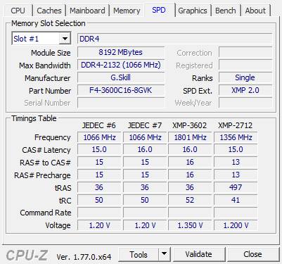
Screenshot 1: Showing the SPD chip readings and memory details.

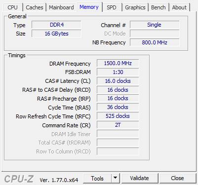
Screenshot 2: Showing the ‘current’ RAM timings , frequency and FSB : RAM ratio.

SECTION 2 : Ram Timings
When it comes to Overclocking RAM we are just concerned with 4(out of many) primary timings as seen in screenshot 2. The chips used on the DDR ram modules have different types of timings(Primary & Secondary) which give us a sense of the speed of ram along with its stability and rated frequency of-course. When it comes to overclocking loosening(increasing) the timings is very effective for increasing the RAM frequency making the modules stable at high frequencies and on the contrary reducing the RAM frequency the timings can be tightened (lowered). But ironically lowering the timings decreases access time but at the cost of the bandwidth.
Now lets get a feel of some of the Signals(strobes) for RAM:
- /CAS[Active low] : Column access strobe(signal) When this signal goes low , the column in the selected row is ready to be accessed in burst mode of 2 , 4 or 8.
- /RAS[Active low] : Row access strobe(signal)
- Precharge : Used to activate/deactivate a row in the selected bank before it can be used for read/write operation.
These timings are specified are in the following order : tCL-tRCD-tRP-tRAS and as you have guessed ‘t’ stands for time.
CAS Latency in ns = CAS delay in cycles x time taken for 1 cycle
But time period is inverse of frequency; Hence we get,
CAS Latency in ns = CAS Latency in cycles x [Bus Frequency] –1
Finally,
CAS LAtency in ns = CAS Latency in cycle / Bus Frequency
The 4 important timings with respect to RAM Overclocking are :
- t-CL [CAS Latency] : It is time elapsed between the memory controller sending the address of the column and the data that “first” arrives in response. Since data is sequentially placed in memory and a row contains sequential data so its quite simple to catch the fact that columns will be switched more frequently than rows so CAS will have a big impact on performance. Though some say that CL is not that important, but generally it is and its only in the case of bizarre memory access patterns that CL may become less significant.
Typical t-CL Values in clock cycles :
- DDR1 – 2,3
- DDR2 – 4 to 6
- DDR3 – 6 to 10
- DDR4 – 10 to 18
- t-RCD [RAS to CAS Delay] : It is the amount of delay between a RAS and a CAS.=or= Simply speaking it is the time taken to select a particular row first and then selecting the particular column for data access. It doesn’t have a huge impact on performance.
Typical t-RCD Values in clock cycles :
- DDR1 – 2 to 4
- DDR2 – 3 to 5
- DDR3 – 6 to 10
- DDR4 – 10 to 18
- t-RP [RAS Precharge Time] : It is the time required to deactivate the current row and activate next row.
=or=
Simply delay caused by switching between rows.Typical t-RP Values in clock cycles :- DDR1 – 2 to 4
- DDR2 – 3 to 5
- DDR3 – 6 to 10
- DDR4 – 10 to 18
- t-RAS [Active to Precharge Delay / Row Active Time] : Time required between an active and a precharge command.
=or=
The time taken between 2 memory access / Data requests.
=or=
The time taken to activate a memory bank(row) and then deactivating it. It affects stability more than performance. It is approximately equal to tCL + rRCD + tRP [=>tRAS] while in some cases it may not be so. And here’s a quote from a wiki article :“in practice for DDR RAM Modules , it should be set to at least tRCD + tCAS + 2 to allow enough time for data to get streamed out”
Typical t-RAS values in cycles :- DDR1 – 5 to 12
- DDR2 – 10 to 19
- DDR3 – 15 to 30
- DDR4 – 20 to 36
SECTION 3A : FSB:DRAM Ratio on Legacy Systems
In case of legacy systems where the memory controller was present on the northbridge, while talking about FSB : DRAM ratio we are concerned with the base FSB frequency and the DRAM frequency (base clock rate).This ratio tells us “who is running faster than whom” and when DRAM frequency is more than base FSB or both are the same then we won’t have any issues with system performance. Depending on both the frequencies, FSB : DRAM ratio can yield any one of the 2 operating modes which are Synchronous and Asynchronous.
Synchronous Mode: (sync)
- In sync mode both the frequencies are equal which means that both the RAM and FSB are running synchronously and yields max performance.
Asynchronous Mode: (async)
- Note that Async mode can give either max performance or average performance as follows:
- If the FSB frequency is more than DRAM frequency then u’ll get average or poor performance because FSB(hence CPU) is running faster than RAM and so RAM cannot cope with data hungry CPU’s requests and eventually CPU has wait i.e be in a idle state for a while till the data arrives from RAM.
- If the DRAM frequency is more or equal to FSB clock speed then u’ll get max performance since here CPU doesn’t have be idle in between and also DRAM being faster than FSB is not a concern since CPU will read/write data at FSB’s rate.
Common FSB ratios :
- 3:4 -> For each 4 DRAM ticks , FSB ticks at rate of 3
- 2:3 -> FSB is at 266 Mhz and DRAM is at 400 Mhz
- 1:1 -> Both are equal for e.g both running …at say 266 Mhz
- 5:4 -> You can guess this!
SECTION 3B : FSB:DRAM Ratio on current Systems
On Current systems be it Intel or AMD where the Memory controller is integrated completely inside the CPU die, the significance of FSB:DRAM ratio has changed. What we used to call FSB is now QPI(Quick path interconnect) on Intel systems and for AMD systems we call it HyperTransport(HT). Now its just a ratio of Base Clock (BCLK) to Memory Clock.
SECTION 4 : Ram Voltages
This is the last thing you wanna mess with , after it being configured according to the EPP or XMP profile. Generally voltage increase must be limited to 8% to 10% of the max supported voltage according to EPP or XMP Profile and you must make sure that the chips on the RAM modues supports this level of voltage increment else you will end up damaging it. For DDR2 for Mobos which support Core2 architecture 2.1/2.2/2.3 V is safest maximum but this doesn’t mean all RAMs have this as their max safe limit. The safest max voltage depends on the chips used by the manufacturer. For DDR2 generally the default is 1.8V while for DDR3 its 1.5V . It again majorly depends on the chips used for the modules. But i’d say never-ever do this until you have enough experience and know about various chips. Instead set the RAM’s voltage according to EPP/XMP profile if not set.
Standard JEDEC & Oveclocked Voltages :
- For DDR1 – Jedec = 2.5V | OC = 3.2v Max
- For DDR2 – Jedec = 1.8V | OC = 2.3V Max , 1.8V~2.2V is ‘just safe’ for 24/7
- For DDR3 – Jedec = 1.5V | OC = 2.1V Max , 1.5~2.0V is ‘just safe’for 24/7 while on some systems 1.65V+ may be fatal (old corei7 LGA1366 systems).
- For DDR4 – Jedec = 1.2V | OC = 1.35v-1.40v Max , 1.2~1.35V is ‘just safe’for 24/7 while it seems that going over1.5V might be serious risky stuff.
SECTION 5 : A Word On SPD & XMP/EPP Profiles
SPD is the acronym for Serial Presence Detect. SPD chips are now commonly found on the SDRAM DIMM Modules. Its job is to store the RAM settings for different frequency and voltages. SPD makes it easier for bios to configure RAM for the system. Apart from the JEDEC standard profiles SPD also contains EPP or XMP profiles. EPP is Enhanced Performance Profile which can be read by some Nvidia and AMD chipsets and configures the RAM according to it. If not supported then BIOS just loads the default configuration. EPP is present on RAM modules which are marketed as “SLI ready” or “Crossfire ready” which is just a marketing thing then any thing else. If the Motherboard cannot read EPP it does not mean that the RAM cannot be configured as per the EPP. In this case we just have to configure it manually. XMP is Intel’s substitute for EPP which is short for eXtreme Memory Profile.
The use of EPP/XMP is just to get the RAM configured for max performance at its rate specifications which are often beyond the standard Jedec specs for Overclocking grade RAMs. When you first install High-speed memory sticks, they will run at ‘default’ Jedec speeds. To configure your RAM sticks at the rated speed you will have enter BIOS and apply the XMP profile. This setting is usually present under the Overclocking/Tweaking section of your BIOS. Many RAM sticks have multiple XMP profiles; so just choose the best one available, which will provide a baseline setting for overclocking. Screenshot-1 shows SPD profiles of my RAM.
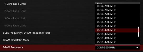
Here is my BIOS screenshot showing XMP profiles available to select from:

SECTION 6 : How do we do it?
After getting equipped with the knowledge presented above its time to do some RAM Overclocking which is straight forward.
I like to do it in 2 cycle fashion:
CYCLE A: Find your Overclock settings at rated Voltage.
CYCLE B: Find your max Overclock at bumped up Voltages past your Overclock at rated Voltages.
The following Steps Integrate both these Cycles:
-
Pre-requisite : If applicable, First apply the XMP/EPP profile for your RAM from BIOS.
- 1) Now, Increase the frequency to next available increment from the list. This setting is usually called “DRAM frequency”. On Some systems it may be called “Memory multiplier” where you will need to select the next multiplier value in the list. You can fine tune the values of these increments by changing the FSB or BaseClock as mentioned in STEP 8.

- 2) If the system is stable then, run all the necessary stability tests.
- 3) If tests are successful repeat step 1.
- 4) If tests fail i.e. system crashes(unstable) during testing then loosen(increase) the timings. You can increase the 4 timings mentioned above by 1-1-1-2 or 1-1-1-3 receptively and repeat until you get stability.

- 5) Now start again from step 2.
- 5.1) Some where here you must get a stable overclock. Now if you want you can repeat the process again from Step 1.
- 6) If you want to Overclock memory further and/or if system crashes after step 5 its time to increase voltage – AT YOUR OWN RISK!
- 7) Increment DRAM voltage in steps of 0.05v or 0.02v depending on your memory module [BEWARE].
- 7.1) If system is unstable or if sometimes you get: “Overclocking failed” in BIOS during boot then, it may be time to increase IO voltage. This is essentially the memory controller voltage. On Current systems(CPU with IMC) its generally called VCCIO in most BIOSes. On Legacy systems its the Northbridge Voltage or NB Voltage. Initially try with 1% to 2% bumps. Consult the Motherboard manual and/or CPU datasheet for absolute max IO Voltage. Its better to ask experienced fellow Overclockers who own the same(nearly) system as your.
- 7.2) You can stop after step 7 or proceed further for some more insanity.
- 8) You can adjust your FSB or Base Clock(BCLK) and repeat from step 2 =or= step 1 for memory frequency fine tuning. On some systems (before Skylake) the Base Clock is tied to PCIE & DMI, hence you don’t have much headroom to overclock your Base Clock(BLCK). If not obvious, please note that increasing your base clock will also increase your CPU speed.
- 9) After this you would have pushed your RAM to its limits and a little more OCing would seriously damage your RAM or even worse your CPU with integrated memory controller..
RAM stability test and other Utilities:
- http://www.memtest86.com/
- http://hcidesign.com/memtest/
- Prime95 – for CPU Benchmarking & stability test | Link : http://mersenne.org
- CPUZ – Gives you all your hardware info | Link : http://cpuid.org
